Inter-metal dielectric of semiconductor device and manufacturing method thereof

a technology of metal dielectric and semiconductor device, which is applied in the direction of semiconductor device, semiconductor/solid-state device details, electrical apparatus, etc., can solve the problems of copper line layer corrosion or adhesion failure, peeling or delamination of copper line layer, etc., and achieves high mobility

Inactive Publication Date: 2006-06-29
DONGBU ELECTRONICS CO LTD
View PDF5 Cites 2 Cited by
  • Summary
  • Abstract
  • Description
  • Claims
  • Application Information

AI Technical Summary

Benefits of technology

[0015] In the present invention, a passivation layer is formed on the PEFSG layer by plasma treatment, so the peeli...

Problems solved by technology
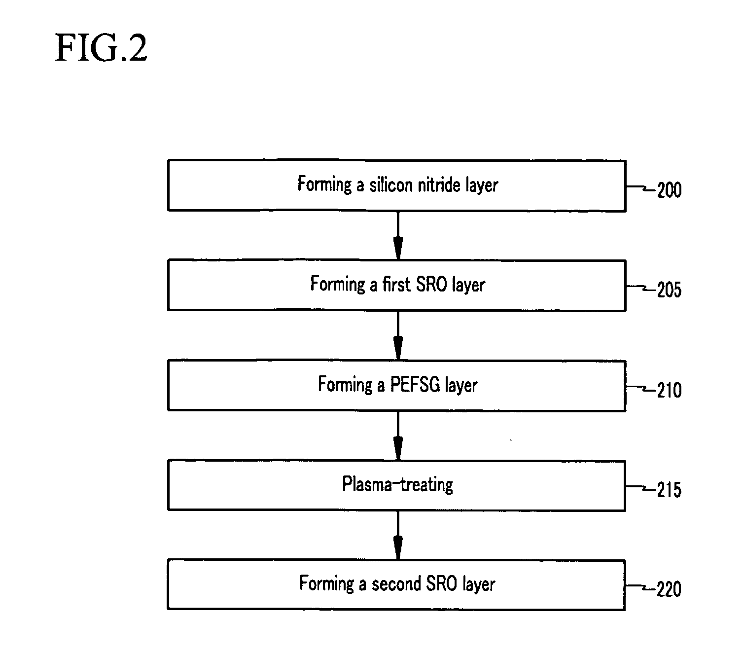
The hydrofluoric acid (HF) may cause corrosion of the copper line layer or adhesion failure thereof.
The adhesi...

Method used


Image

  • Inter-metal dielectric of semiconductor device and manufacturing method thereof
  • Inter-metal dielectric of semiconductor device and manufacturing method thereof
  • Inter-metal dielectric of semiconductor device and manufacturing method thereof

Examples


Embodiment Construction

[0019] An exemplary embodiment of the present invention will hereinafter be described in detail with reference to the accompanying drawings.

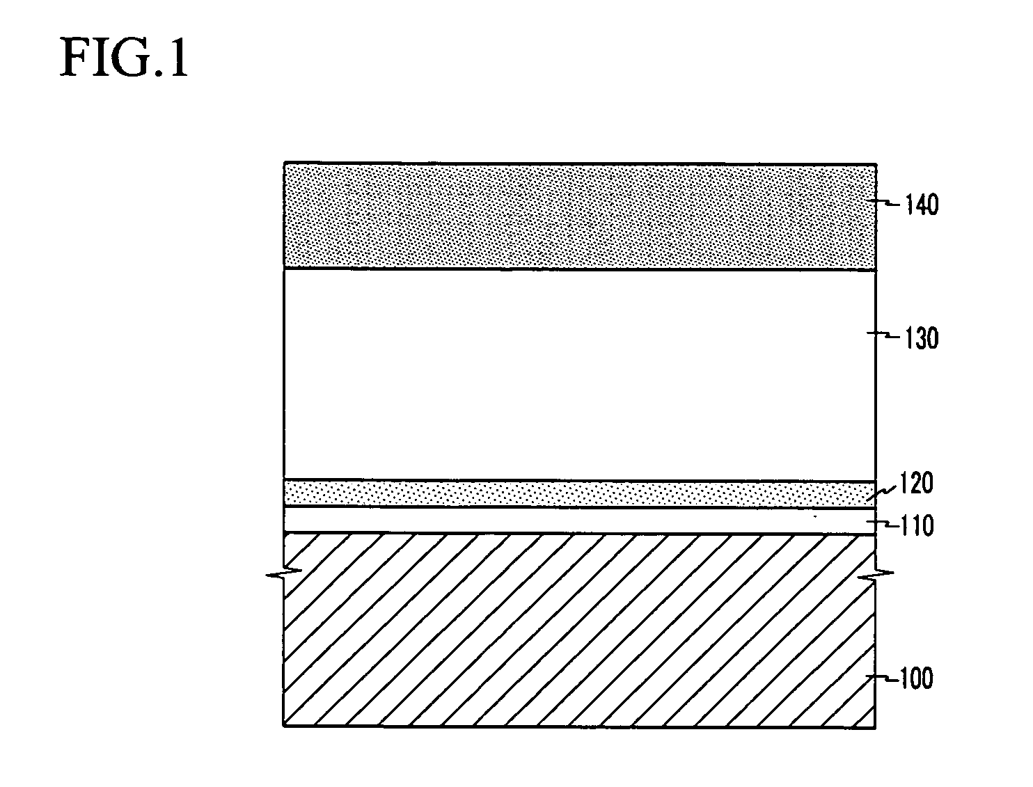
[0020]FIG. 1 is a cross-sectional view showing a conventional inter-metal dielectric of a semiconductor device.

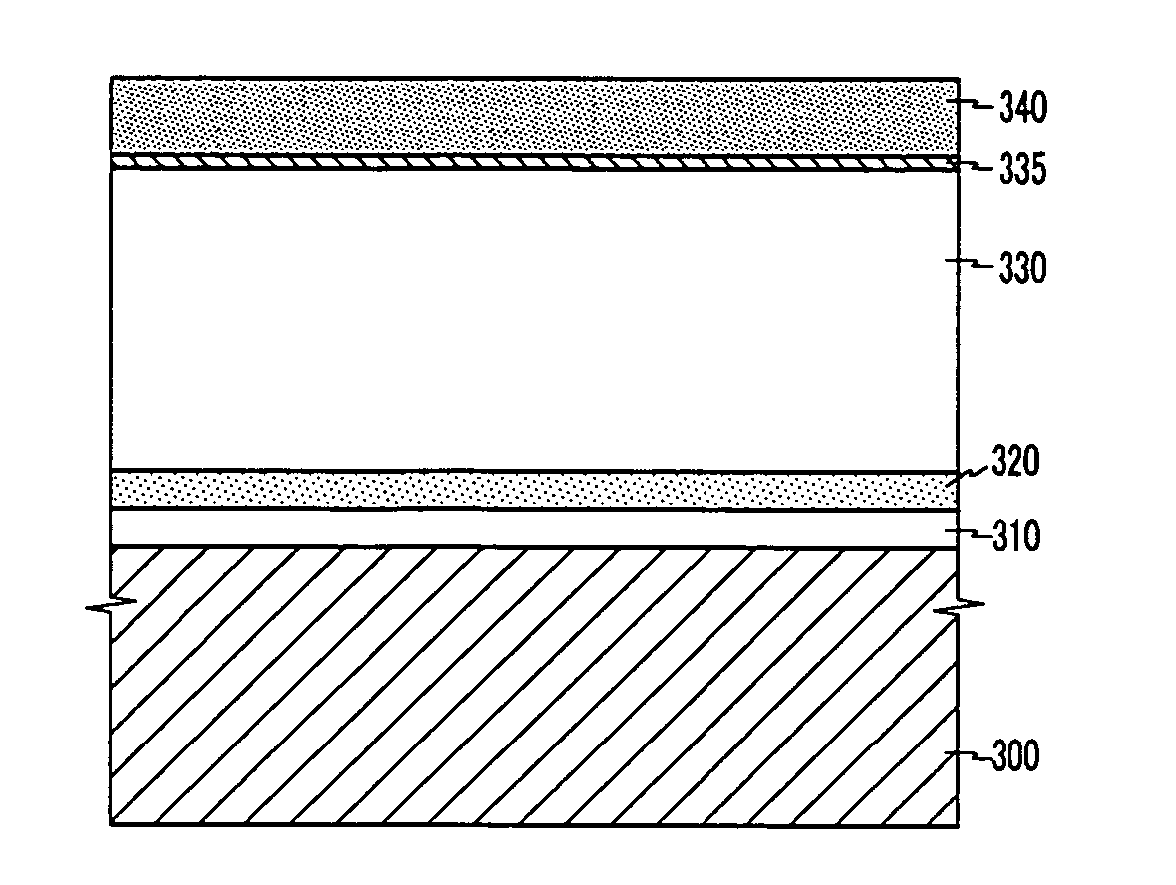
[0021] An inter-metal dielectric for a copper damascene process includes a silicon substrate 100 provided with a copper line layer therein (not shown, but generally, a conventional single or dual damascene copper metallization layer), a silicon nitride layer 110 (e.g., an etch-stop layer) thereon, a fluorosilicate glass (FSG) layer 130 having a low dielectric constant, and a pair of silicon rich oxide (SRO) layers 120 and 140 configured to prevent fluorine-outgassing from FSG layer 110. Silicon rich oxide (SRO) layers 120 and 140 are respectively formed beneath and above the FSG layer 130. The upper SRO layer 140 may have a thickness of 2000-3000 Å, so the total dielectric constant of the inter-metal dielectric may be enhanced. Theref...


PUM


Abstract

An exemplary manufacturing method of an inter-metal dielectric of a semiconductor device according to an embodiment of the present invention includes forming a first silicon-rich oxide (SRO) layer on a silicon substrate provided with or otherwise having a copper line layer therein, forming a plasma enhanced fluorosilicate glass (PEFSG) layer on the first SRO layer, plasma-treating the PEFSG layer, and forming a second SRO layer on the plasma-treated PEFSG layer. According to the present invention, the thickness of the second SRO layer of the inter-metal dielectric can be reduced. Consequently, process cost can be reduced, and the total thickness of the inter-metal dielectric can be reduced so as to lower the dielectric constant thereof, reduce the aspect ratio of any via holes that are subsequently formed in the inter-metal dielectric, and potentially increase the yield as a result of the reduced via hole aspect ratio.

Description

CROSS-REFERENCE TO RELATED APPLICATION [0001] This application claims priority to and the benefit of Korean Patent Application No. 10-2004-0111041, filed in the Korean Intellectual Property Office on Dec. 23, 2004, the entire contents of which are incorporated herein by reference. BACKGROUND OF THE INVENTION [0002] (a) Field of the Invention [0003] The present invention relates to a dielectric in a semiconductor device and a manufacturing method thereof. More particularly, the present invention relates to an inter-metal dielectric of a semiconductor device using a copper damascene process and a manufacturing method thereof. [0004] (b) Description of the Related Art [0005] Materials having low dielectric constants have been generally used as inter-metal dielectrics for aluminum and copper damascene metallization in semiconductor devices, so that the RC delay time of the devices can be reduced, and the performance of the devices can be enhanced. Fluorosilicate glass (FSG) having a die...

Claims


Application Information

Patent Timeline
IPC IPC(8): H01L21/44H01L21/31
CPCH01L21/02131H01L21/02274H01L21/02304H01L21/0234H01L21/02362H01L21/3144H01L21/31612H01L21/31629H01L21/76826H01L21/76829H01L21/31
Inventor LEE, TAE-YOUNG
Owner DONGBU ELECTRONICS CO LTD
Why Eureka
Try Eureka