Silicon carbide single crystal and method and apparatus for producing the same

a technology of silicon carbide and single crystal, which is applied in the direction of single crystal growth, polycrystalline material growth, chemistry apparatus and processes, etc., can solve the problems of deterioration of single crystallinity, low single crystal growth rate, and generation of crystal defects and polycrystallization. , to achieve the effect of suppressing the generation of crystal defects and high silicon carbide single crystal growth ra

Inactive Publication Date: 2006-07-06
SHOWA DENKO KK
View PDF11 Cites 19 Cited by
  • Summary
  • Abstract
  • Description
  • Claims
  • Application Information

AI Technical Summary

Benefits of technology

[0022] As described above, in the present invention, by surrounding by an atmosphere gas of silicon carbide a growth crucible provided therein with a seed crystal substrate on which a silicon carbide single crystal is deposited using a sublimate gas of a silicon carbide raw material and maintaining the atmosphere gas pressure higher than the pressure of the silicon gas in the sublimate gas within the growth crucible, the silicon gas diffuses within the growth crucible through the growth crucible wall, thereby enabling the generation of crystal defects to be suppressed to a great extent and a large-sized single crystal to be grown reliably on the seed crystal substrate.
[0023] Particularly by regulating the pressure of the atmosphere gas surrounding the growth crucible to 1.33×10² to 4.0×10⁴ Pa, a high growth rate of the silicon carbide single crystal that is 1 mm / hour or more can be attained.

Problems solved by technology

Therefore, the sublimation process involves the problems in 1) that the growth rate of the single crystal is low and 2) that when the growth rate is increased, generation of crystal defects and polycrystallization tend to occur.
Variation in the composition of the sublimate gas at a region in the vicinity of the surface of the seed crystal substrate on which the single crystal is grown is considered to cause generation of crystal defects in silicon carbide crystals and formation of polytypes or growth of anisotropic crystals (i.e., polycrystallization), which lead to deterioration of crystallinity of the single crystal.
However, these measures are not satisfactory in terms of the quality and stability of a silicon carbide single crystal produced through the sublimation process.
However, this method inevitably involves a fundamental problem associated with the sublimation process, i.e., variation in the composition of the sublimate gas with the progress of sublimation of the silicon carbide.
In addition, in this method, production of a silicon carbide single crystal requires a two-step process, leading to relatively long production time.
However, this method entails a drawback in that the growth rate of the silicon carbide single crystal is low since the vapor pressure of carbon is lower than that of silicon.
As described above, there has not yet been established an effective method for controlling factors causing variation in the composition of a sublimate gas to thereby grow a silicon carbide single crystal of high crystallinity.

Method used


Image

  • Silicon carbide single crystal and method and apparatus for producing the same
  • Silicon carbide single crystal and method and apparatus for producing the same
  • Silicon carbide single crystal and method and apparatus for producing the same

Examples


example 1

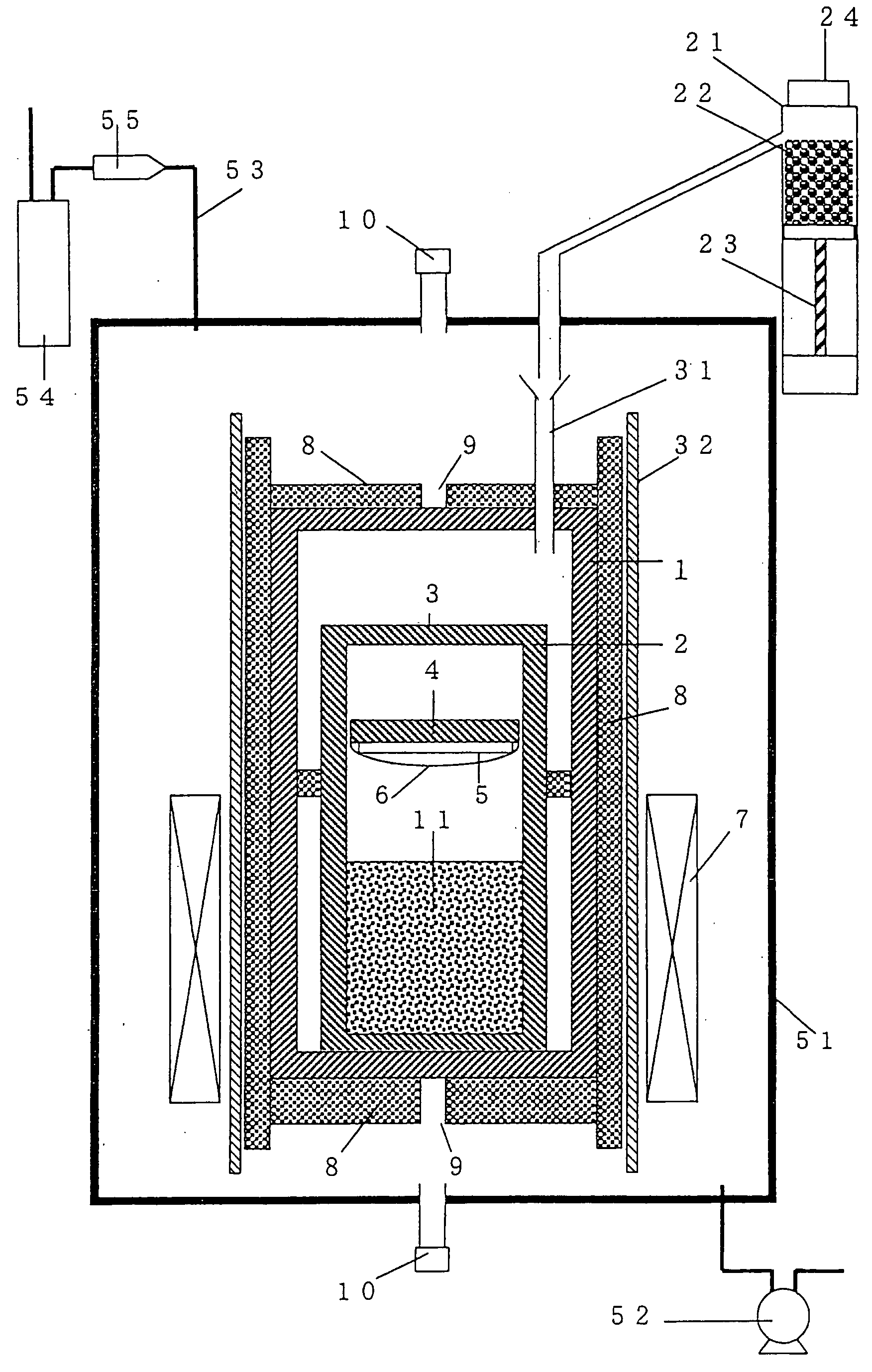
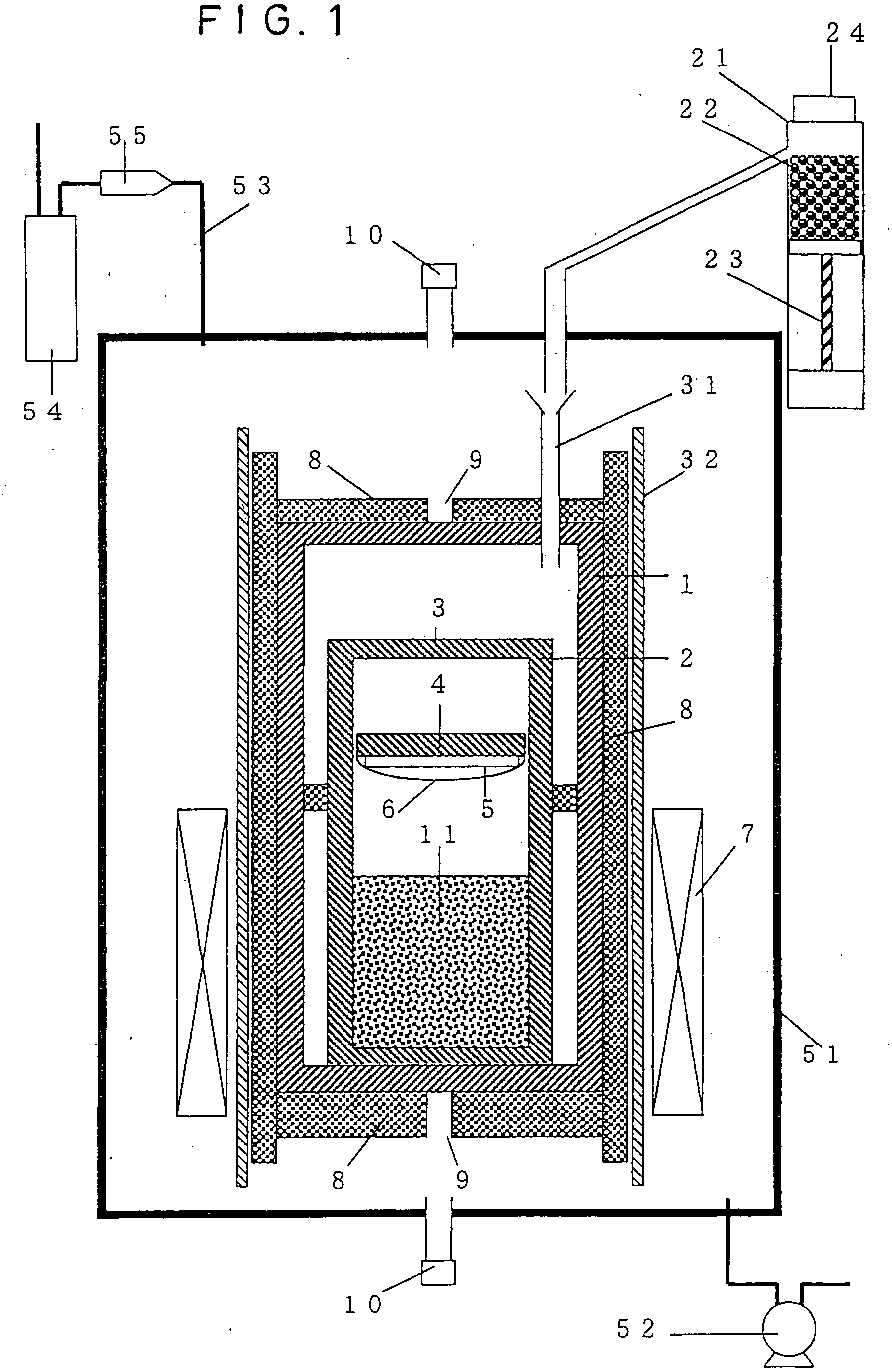
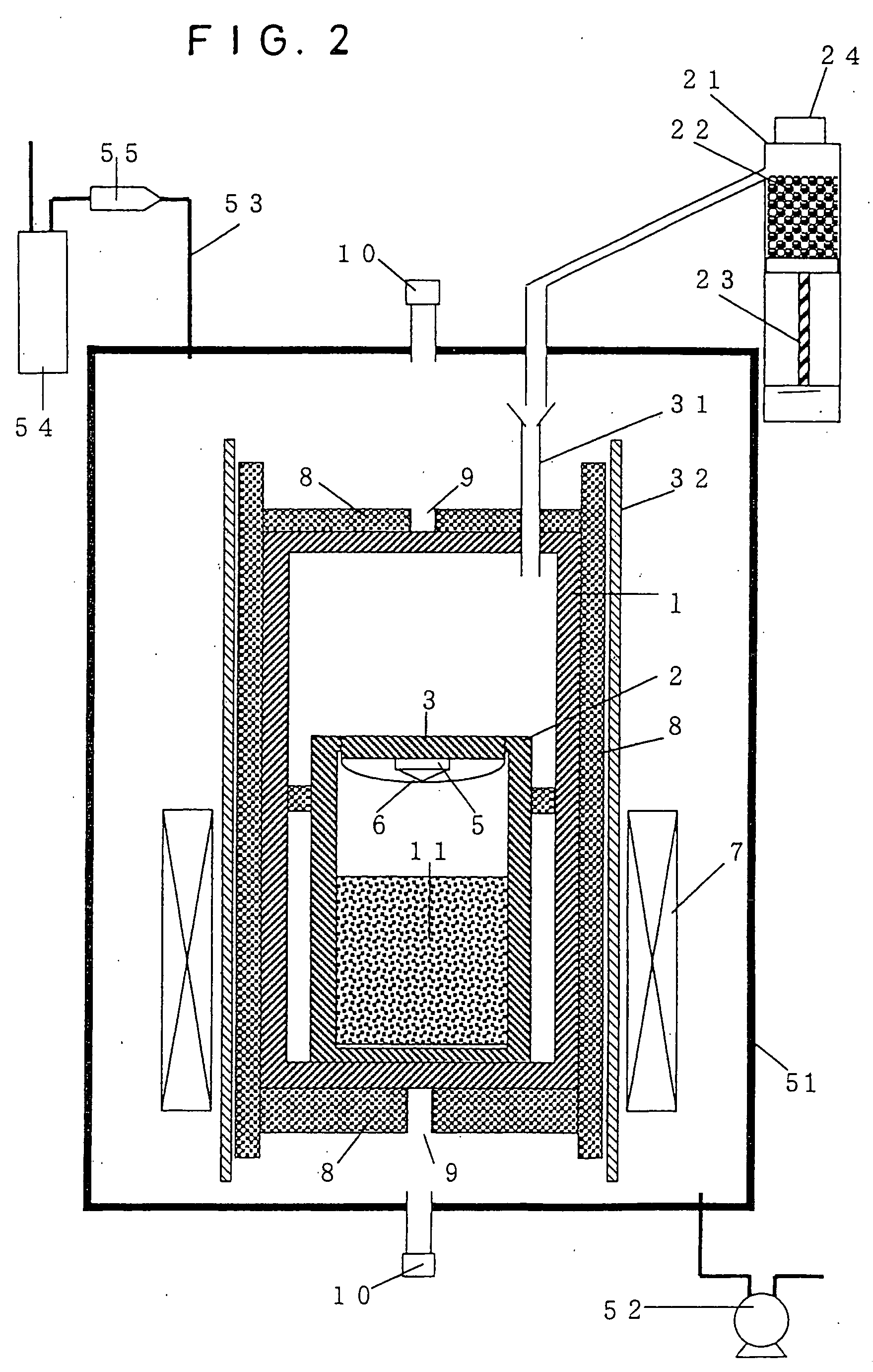
[0054] In Example 1, a silicon carbide single crystal was grown by use of the silicon carbide single crystal production apparatus shown in FIG. 1. Firstly, a seed crystal substrate 40 mm in diameter and 1.0 mm in thickness formed from a 6H-SiC single crystal having a (0001) plane was attached, by means of an adhesion technique, to the center portion of the surface, which faces the bottom of a growth crucible, of a supporter (formed of graphite, thickness: 9 mm) provided in the growth crucible. The growth crucible is formed of a bottomed graphite-made hollow cylinder 52 mm in inner diameter and 116 mm in height. A powdery silicon carbide raw material (about 172 g) was placed in the growth crucible at a height of about 52 mm from the bottom of the crucible. The supporter was provided in the growth crucible such that the lower surface of the seed crystal substrate was located at a position 32 mm distant from the level of the raw material. The growth crucible was placed in the center of...

example 2

[0062] In Example 2, a silicon carbide single crystal was grown using the apparatus shown in FIG. 1, the same crucibles and seed crystal substrate as in Example 1 were employed, and the same growth process as in Example 1 was adopted. However, the temperatures of the lower and upper portions of the outer crucible were maintained at about 2,480° C. and 1,980° C., respectively, and the argon atmosphere in the growth chamber was maintained under a pressure of 1.5×10⁴ Pa during the course of crystal growth. The crystal growth was performed for 5 hours while introducing the silicon raw material into the outer crucible in the same manner as in Example 1.

[0063] The thus grown silicon carbide single crystal was found to have a diameter of about 50 mm at its tip portion and a growth length of 10.5 mm.

[0064] Subsequently, the powdery silicon carbide raw material in the growth crucible was exchanged to a fresh one, and a silicon carbide single crystal was then grown on the above grown crysta...


PUM

PropertyMeasurementUnit
diameteraaaaaaaaaa
temperatureaaaaaaaaaa
pressureaaaaaaaaaa

Abstract

A growth crucible (2) for depositing on a seed crystal substrate (5) a silicon carbide single crystal (6) using a sublimate gas of a silicon carbide raw material (11) is disposed inside of an outer crucible (1). During the course of silicon carbide single crystal, a silicon raw material (22) is continuously fed from outside into a space between the growth crucible and the outer crucible for the purpose of vaporizing the silicon raw material. An atmosphere gas surrounding the growth crucible is constituted of a silicon gas. The pressure of the atmosphere silicon gas is controlled to suppress a variation in the composition of the sublimate gas within the growth crucible to thereby grow a large-sized silicon carbide single crystal with few crystal defects on the seed crystal substrate reliably at a high growth rate.

Description

CROSS REFERENCE TO RELATED APPLICATIONS [0001] This application is an application filed under 35 U.S.C. §111(a) claiming the benefit pursuant to 35 U.S.C. §119(e) (1) of the filing date of Provisional Application Ser. No. 60 / 414,659 filed Oct. 1, 2002 pursuant to 35 U.S.C. §111(b).TECHNICAL FIELD [0002] The present invention relates to a silicon carbide (SiC) single crystal and to a method and apparatus for producing the silicon carbide single crystal. More particularly, the present invention relates to a method for producing a large-sized silicon carbide single crystal of high quality containing few crystal defects, e.g., micropipes. BACKGROUND ART [0003] Silicon carbide single crystal, which has become of interest as a semiconductor material, is generally produced through a sublimation process employing silicon carbide powder serving as a raw material. In the sublimation process, the silicon carbide powder and a seed crystal substrate are placed in the interior of a graphite-made ...

Claims


Application Information

Patent Timeline
Patent Type & Authority Applications(United States)
IPC IPC(8): C30B23/00C30B25/00C30B28/12C30B28/14
CPCC30B29/36C30B23/00C30B23/002
Inventor SAKAGUCHI, YASUYUKITAKAGI, ATSUSHIOYANAGI, NAOKI
Owner SHOWA DENKO KK
Why Eureka
Try Eureka