Method for forming LOCOS layer in semiconductor device

Inactive Publication Date: 2006-07-06
DONGBU ELECTRONICS CO LTD
View PDF2 Cites 14 Cited by
  • Summary
  • Abstract
  • Description
  • Claims
  • Application Information

AI Technical Summary

Benefits of technology

[0009] An object of the present invention is to provide a method for forming a LOCOS layer in a semiconductor device, by which th

Problems solved by technology

In this case, however, the length of a current transfer path from a source 30 to a drain 40 is increased, the

Method used


Image

  • Method for forming LOCOS layer in semiconductor device
  • Method for forming LOCOS layer in semiconductor device
  • Method for forming LOCOS layer in semiconductor device

Examples


Example

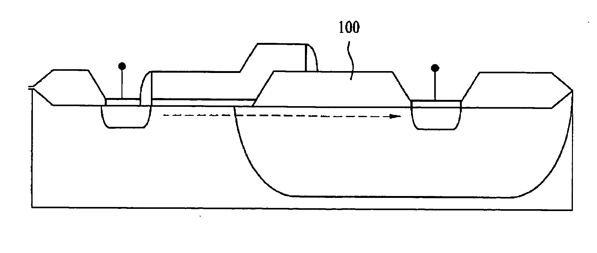
[0017] Reference will now be made in detail to exemplary embodiments of the present invention, examples of which are illustrated in the accompanying drawings. Wherever possible, like reference designations will be used throughout the drawings to refer to the same or similar parts.

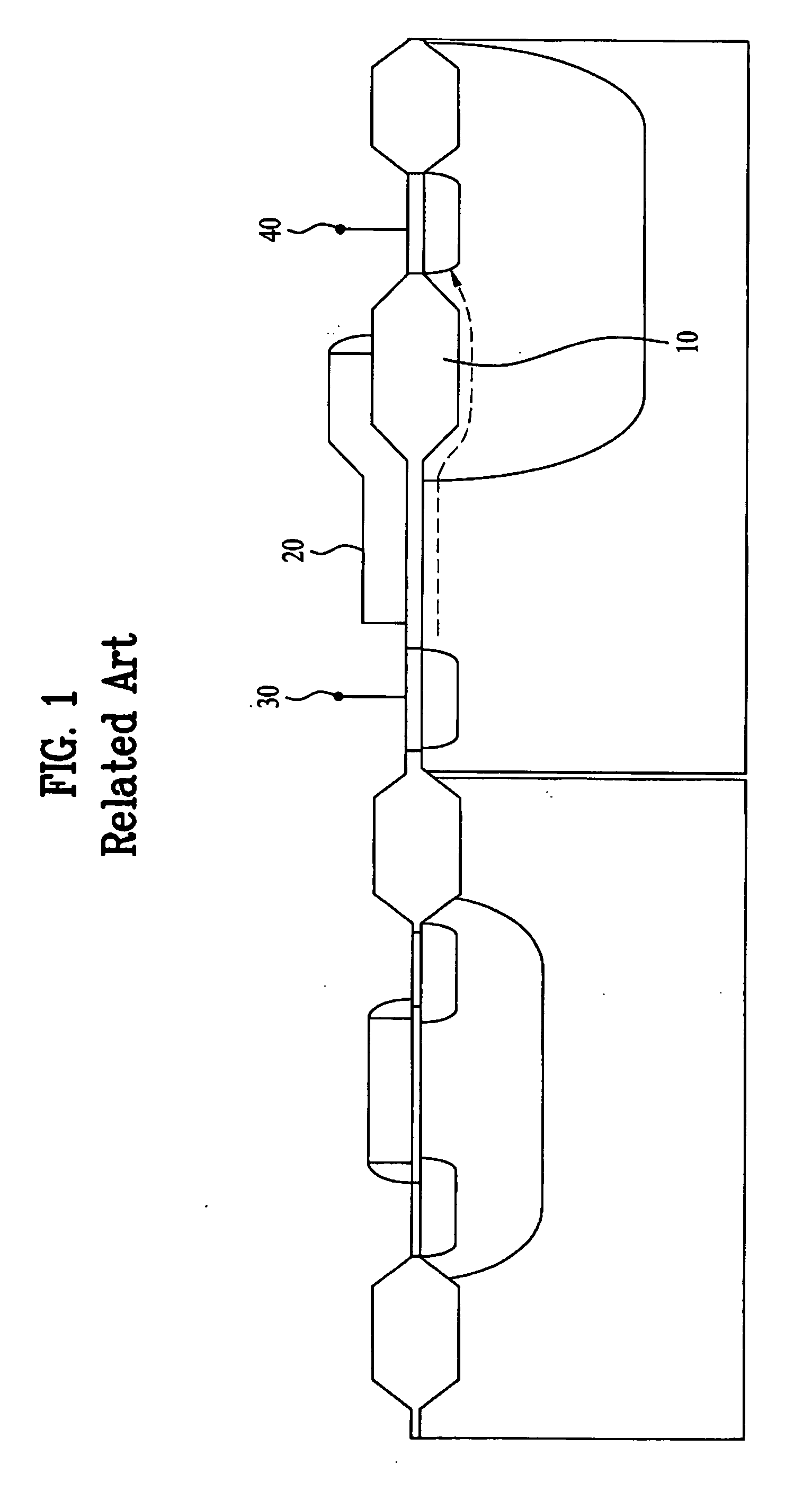
[0018] High voltages are typically applied to a double-diffused MOS (DMOS) or lateral DMOS transistor. In such devices, if the source-to-drain current path can be made shorter, the device's on-state resistance may be reduced and its current driving capability may be enhanced.

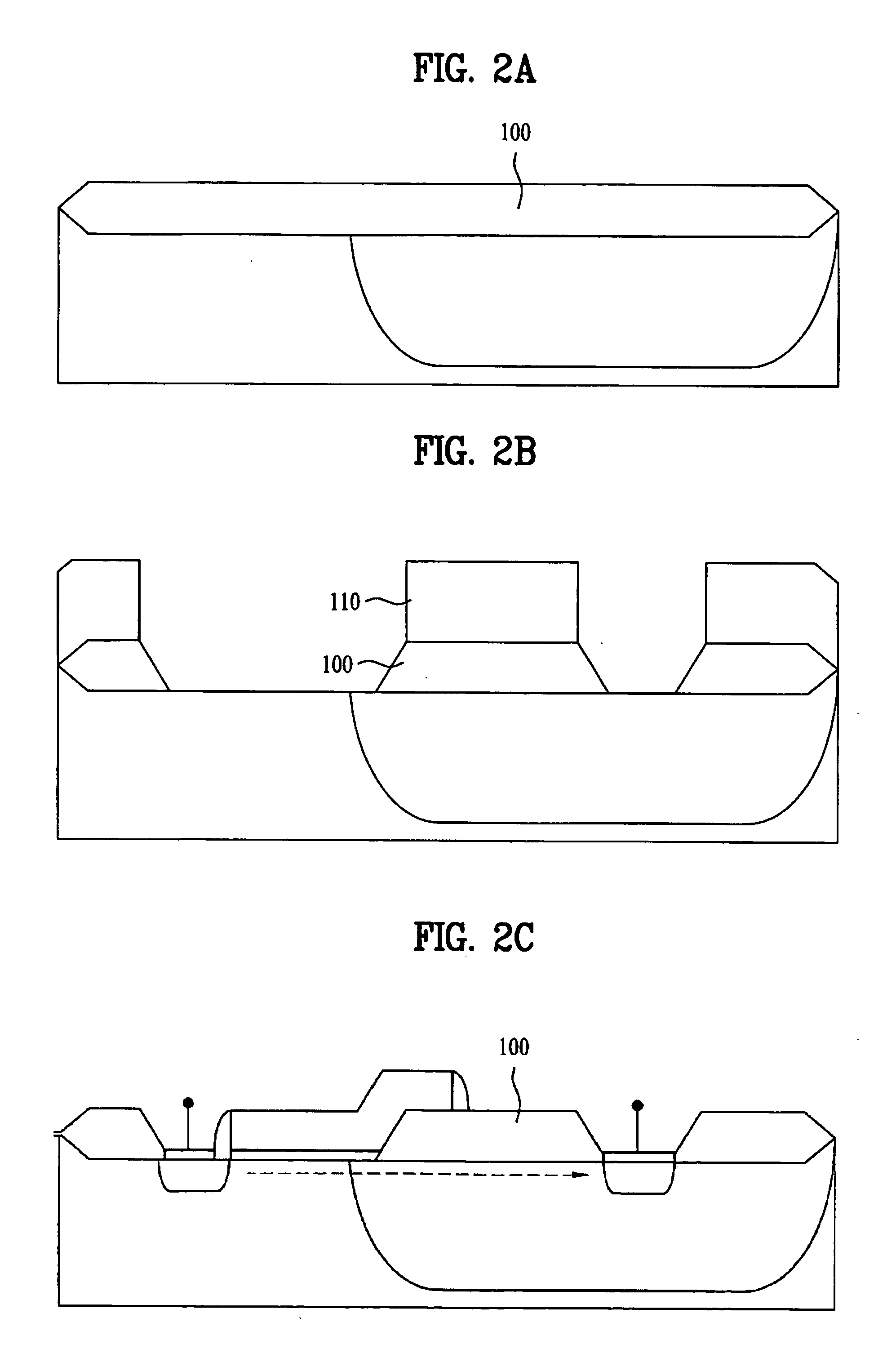
[0019]FIGS. 2A-2C respectively illustrate steps of a method for forming a LOCOS layer in a semiconductor device in accordance with the present invention.

[0020] As shown in FIG. 2A, a silicon oxide layer (e.g., a “pad oxide”) is deposited or grown on a semiconductor substrate having p-type impurities therein. Then, the silicon oxide layer is coated with a first layer of photoresist, which is developed via an exposure step using a mask...


PUM


Abstract

A method for forming a LOCOS layer in a semiconductor device includes steps of oxidizing a high voltage region of the semiconductor device to form a LOCOS layer in the high voltage region; and etching the LOCOS layer according to a pattern.

Description

[0001] This application claims the benefit of Korean Patent Application No. 10-2004-0118290, filed on Dec. 31, 2004, which is hereby incorporated by reference as if fully set forth herein. BACKGROUND OF THE INVENTION [0002] 1. Field of the Invention [0003] The present invention relates to a method for forming a LOCOS layer in a semiconductor device, and more particularly, to a method for forming a LOCOS layer in a semiconductor device, by which the LOCOS layer is etched in a high voltage region to reduce on-state resistance. [0004] 2. Discussion of the Related Art [0005] A system with a single semiconductor chip has improved with an increase in the integration of semiconductor diodes and other devices and with design techniques that have developed as a result. The single chip system may integrate a controller, a memory, and other circuitry, which operate at relatively low voltages. To achieve greater miniaturization, however, the chip may also integrate circuitry for power source co...

Claims


Application Information

Patent Timeline
IPC IPC(8): H01L21/00
CPCH01L21/7621H01L29/42368H01L29/66659H01L29/7835H01L21/76
Inventor SUNG, WOONG JE
Owner DONGBU ELECTRONICS CO LTD
Why Eureka
Try Eureka