Parallel-beam scanning for surface patterning of materials

a scanning and material technology, applied in the field of manufacturing, can solve the problems of insufficient scanning technique, inability to address these problems, and relating to precise and controllable patterning, and achieve the effect of efficient diffusion of dopan

Inactive Publication Date: 2006-07-13
SEMICUBE
View PDF12 Cites 99 Cited by
  • Summary
  • Abstract
  • Description
  • Claims
  • Application Information

AI Technical Summary

Problems solved by technology

However, these approaches have various problems relating to precise and controllable patterning when divergent beams are employed, specifically as regards scanning a plane surface.
For example, galvanometer laser beam scanners, e.g., such as those provided by Cambridge Technology Inc., are well known but do not address these problems (sufficiently precise control of divergent beams so as to scan a plane surface effectively).
However, this “spherical” scan technique is not adequate for scanning a plane surface; the resulting geometrical distortion is a serious shortcoming of such an arrangement.
Another problem is that in prior dual mirror systems the apparent source position is not fixed.
In prior art systems, this effect is generally detrimental to accurate beam positioning on the target.
This configuration attempts to solve the apparent-source-motion problem but still uses diverging beams and thus does not solve the problem of geometrical distortion on a plane surface, e.g., due to non-normal incidence of the beam on the target.
In other words, this approach also suffers from the “spherical” scanning issue described above.
However, such broad illumination of the masked surface requires very powerful beam sources, which are substantially expensive and dangerous.

Method used


Image

  • Parallel-beam scanning for surface patterning of materials
  • Parallel-beam scanning for surface patterning of materials
  • Parallel-beam scanning for surface patterning of materials

Examples


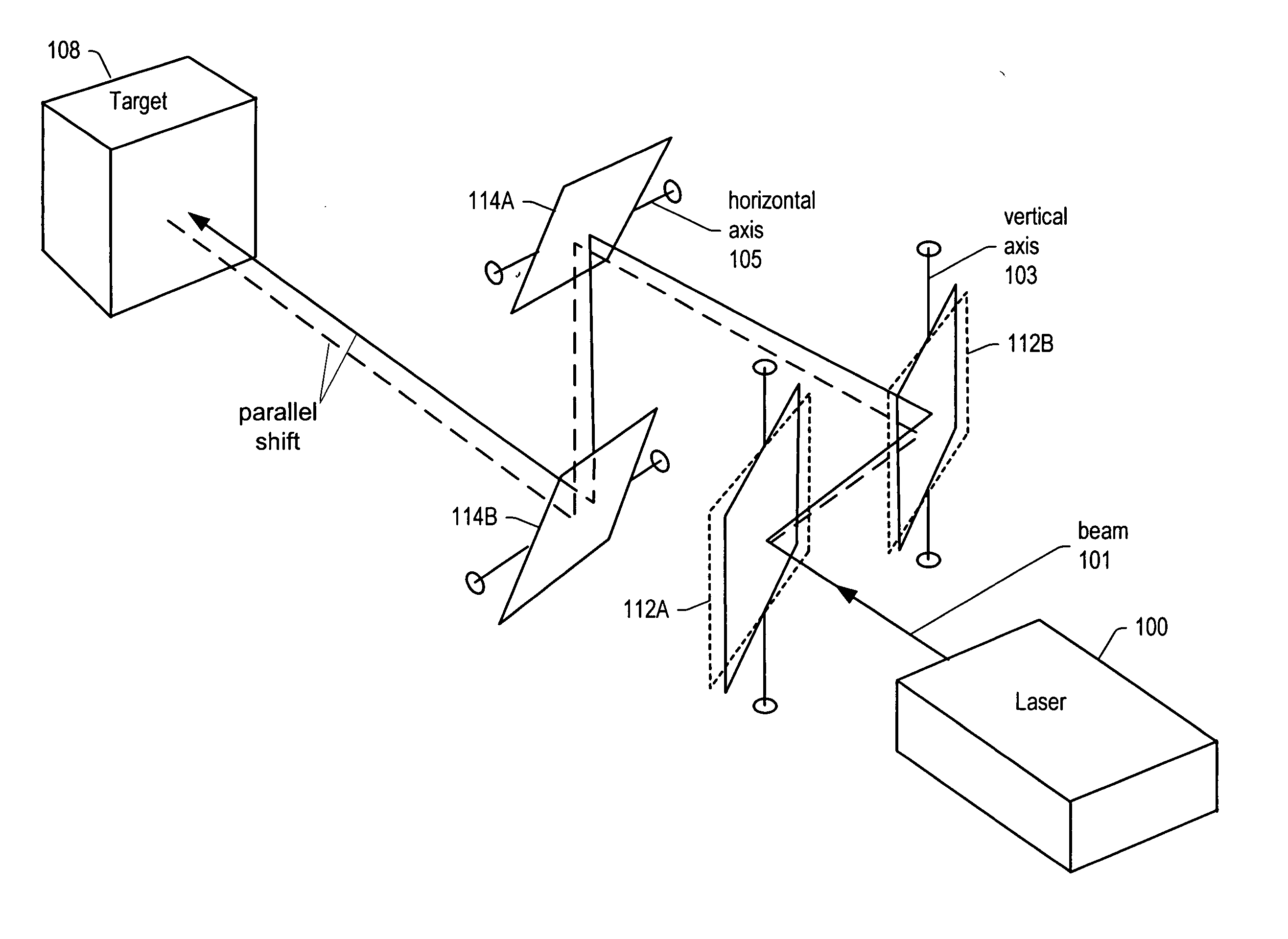
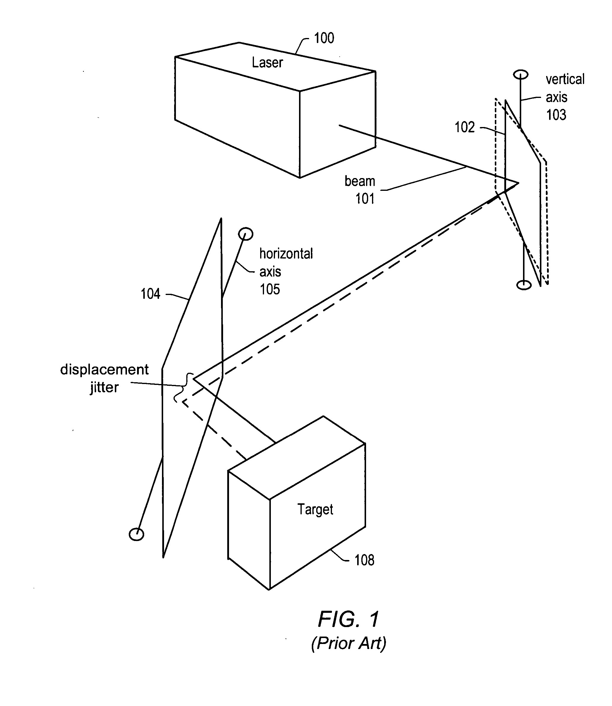
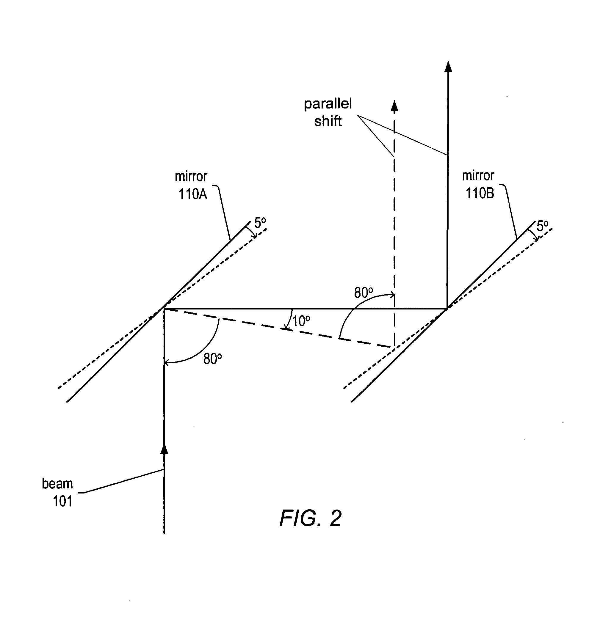
Embodiment Construction

INCORPORATION BY REFERENCE

[0039] The following references are hereby incorporated by reference in their entirety as though fully and completely set forth herein: [0040] U.S. Pat. No. 5,346,850, titled “Crystallization and doping of amorphous silicon on low temperature plastic”, issued on Sep. 13, 1994; [0041] U.S. Pat. No. 6,680,485, titled “Thin film transistors on plastic substrates”, issued on Jan. 20, 2004; [0042] U.S. Pat. No. 6,509,217, titled “Inexpensive, reliable, planar RFID tag structure and method for making same”, issued on Jan. 21, 2003; [0043] U.S. Pat. No. 6,372,592, titled “Self-aligned MOSFET with electrically active mask”, issued on Apr. 16, 2002; [0044] U.S. Pat. No. 5,885,904, titled “Method to incorporate, and a device having, oxide enhancement dopants using gas immersion laser doping (GILD) for selectively growing an oxide layer”, issued on Mar. 23, 1999; [0045] U.S. Pat. No. 5,840,589, titled “Method for Fabricating Monolithic and Monocrystalline All-Semicond...


PUM

PropertyMeasurementUnit
wavelengthaaaaaaaaaa
anglesaaaaaaaaaa

Abstract

A system and method for parallel-beam scanning a surface. An energetic beam source emits an energetic collimated beam which is received by an optical device, comprising: one or more optical media, operable to receive the emitted beam, such as two pairs of coordinated mirrors or a right prism, and at least one actuator coupled to the one or more optical media, and operable to rotate each of the one or more optical media around a respective axis to perform a parallel displacement of the beam in a respective direction, wherein the respective direction, the beam, and the respective axis are mutually orthogonal. The optical device is operable to direct the beam to illuminate a sequence of specified regions of a surface.

Description

FIELD OF THE INVENTION [0001] The present invention relates to the field of manufacture, and more particularly to a system and method for patterning of a surface via an energy beam, such as a semiconductor surface, where the beam causes local heating and may be used to effect local melting of the surface of the material to cause thermally based effects such as dopant diffusion, oxidation, crystallization, and so forth. DESCRIPTION OF THE RELATED ART [0002] Surface patterning refers to the creation or generation of patterns on material surfaces. Many methods have been in use for some time, particularly for surface treatment and patterning of semiconductor wafers. For example, diffusion and ion implantation, rapid thermal processing (RTP), laser etching, reactive ion etching, epitaxial growth, physical and chemical deposition methods based on sputtering, Chemical Vapor Deposition (CVD), and other techniques have been used in conjunction with masks to select the portions of the surface...

Claims


Application Information

Patent Timeline
Patent Type & Authority Applications(United States)
IPC IPC(8): B23K26/00
CPCB23K26/0066B23K26/08B23K26/0807B23K26/4075B23K2201/40G02B26/101B23K26/0081B23K26/0042B23K26/0006B23K26/082B23K26/40B23K26/354B23K26/352B23K2101/40B23K2103/50B23K2103/56
Inventor WARNER, RAYMOND M. JR.MASTERSON, EARL E.MILLAR, LYNNMACCRISKEN, JOHN E.WILLIAMS, MARK S.
Owner SEMICUBE
Why Eureka
Try Eureka