Semiconductor device and power converter, driving inverter, general-purpose inverter and high-power high-frequency communication device using same

a technology of semiconductor devices and power converters, which is applied in the direction of semiconductor devices, basic electric elements, electrical equipment, etc., can solve the problems of increased roughness of silicon carbide surfaces, increased leak current, and reduced channel mobility, so as to improve the electrical characteristics of semiconductor devices and suppress roughness

Inactive Publication Date: 2006-07-13
NAT INST OF ADVANCED IND SCI & TECH
View PDF4 Cites 29 Cited by
  • Summary
  • Abstract
  • Description
  • Claims
  • Application Information

AI Technical Summary

Benefits of technology

[0009] Thus, in each of the above prior-art references, a semiconductor device having a p type or n type region formed on a silicon carbide substrate by impurity ion implantation, is formed on the (0001) face. However, a silicon carbide substrate has various surface orientations, and by contriving the surface orientation and the impurity heat treatment method in that surface orientation, it is possible to suppress the roughness on the silicon carbide substrate surface following the impurity activation heat treatment, improving the electrical characteristics of the semiconductor device.
[0012] This invention is proposed in view of the above, and has as its object, in a semiconductor device that uses a silicon carbide substrate having p type, n type semiconductor impurity regions formed by ion implantation, to improve the ultimate electrical characteristics of the semiconductor device by reducing surface roughness of the silicon carbide substrate.

Problems solved by technology

In this case, when forming a p type or n type region by ion implantation in the (0001) face, ion implantation of a p type or n type impurity is followed by heat treatment at a high temperature of 1500° C. or above for activation, so silicon evaporates from the silicon carbide surface, leading to increased roughness of the silicon carbide surface.
This results in reduced channel mobility of metal-insulation film-semiconductor field-effect transistors (MISFETs) or metal-semiconductor field-effect transistors (MESFETs), and increased leak current in Schottky barrier diodes (SBDs) and junction type field-effect transistors (JFETs) caused by larger crystal defects in the ion implantation region, problems which make practical use impossible.

Method used


Image

  • Semiconductor device and power converter, driving inverter, general-purpose inverter and high-power high-frequency communication device using same
  • Semiconductor device and power converter, driving inverter, general-purpose inverter and high-power high-frequency communication device using same
  • Semiconductor device and power converter, driving inverter, general-purpose inverter and high-power high-frequency communication device using same

Examples


Embodiment Construction

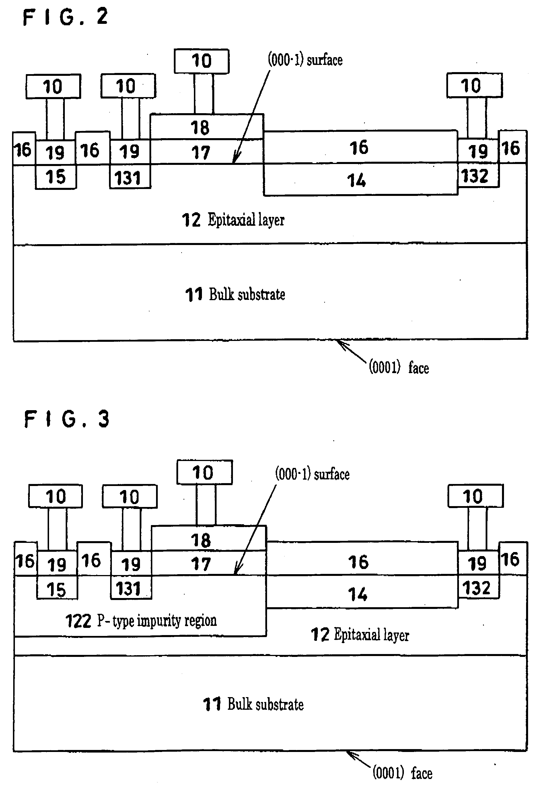
[0021] A method of manufacturing a Schottky barrier diode, a lateral type MIS field-effect transistor and a vertical type MIS field-effect transistor that are examples of a semiconductor device formed using the (000-1) surface of a silicon carbide substrate will be described. This will be followed by showing the results of measurements, by an atomic force microscope, of the surface roughness of substrates that have been heat-treated following ion implantation in the (0001) face used in a semiconductor device that uses a normal silicon carbide semiconductor substrate and in the (000-1) surface proposed by the present invention.

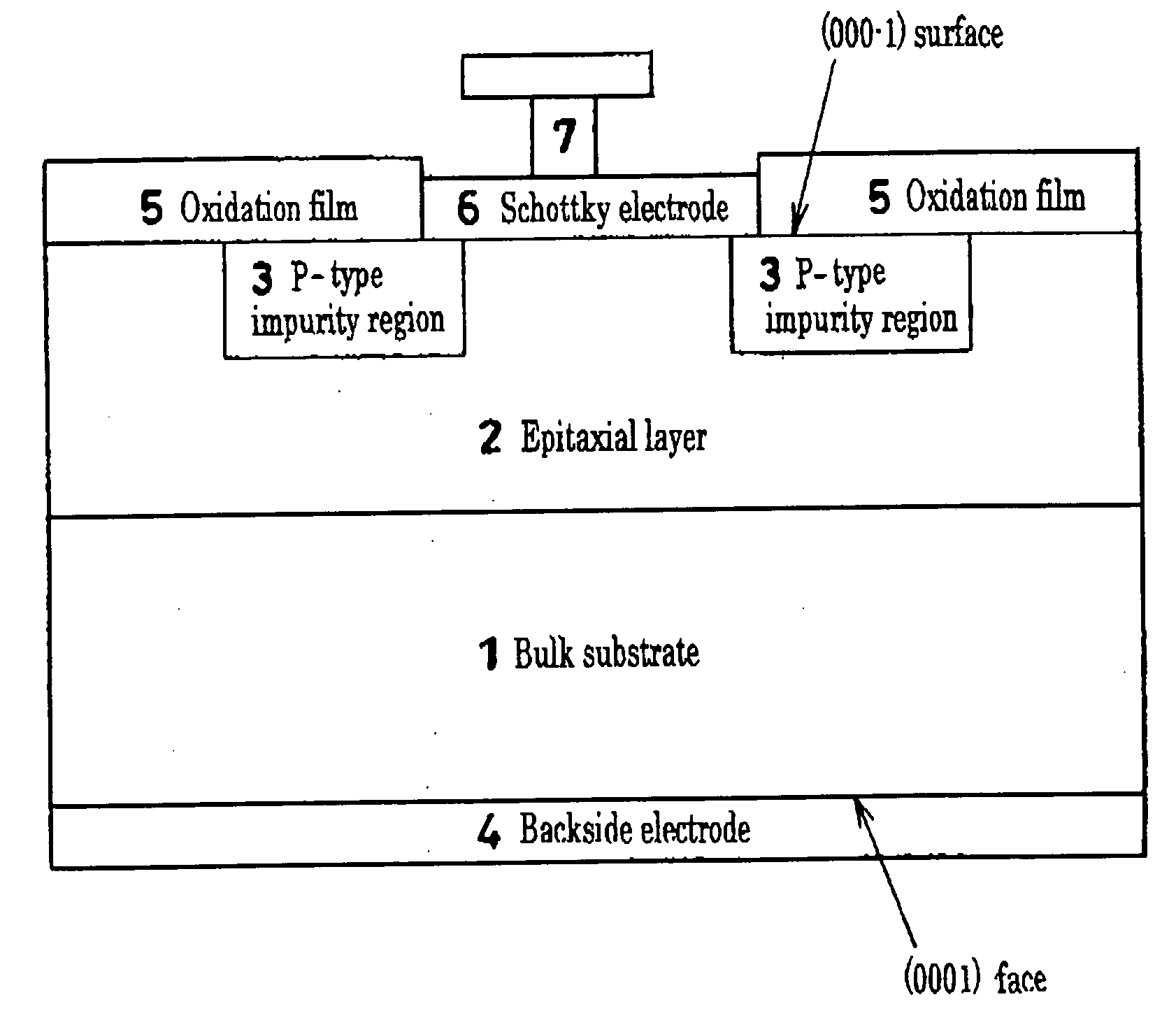
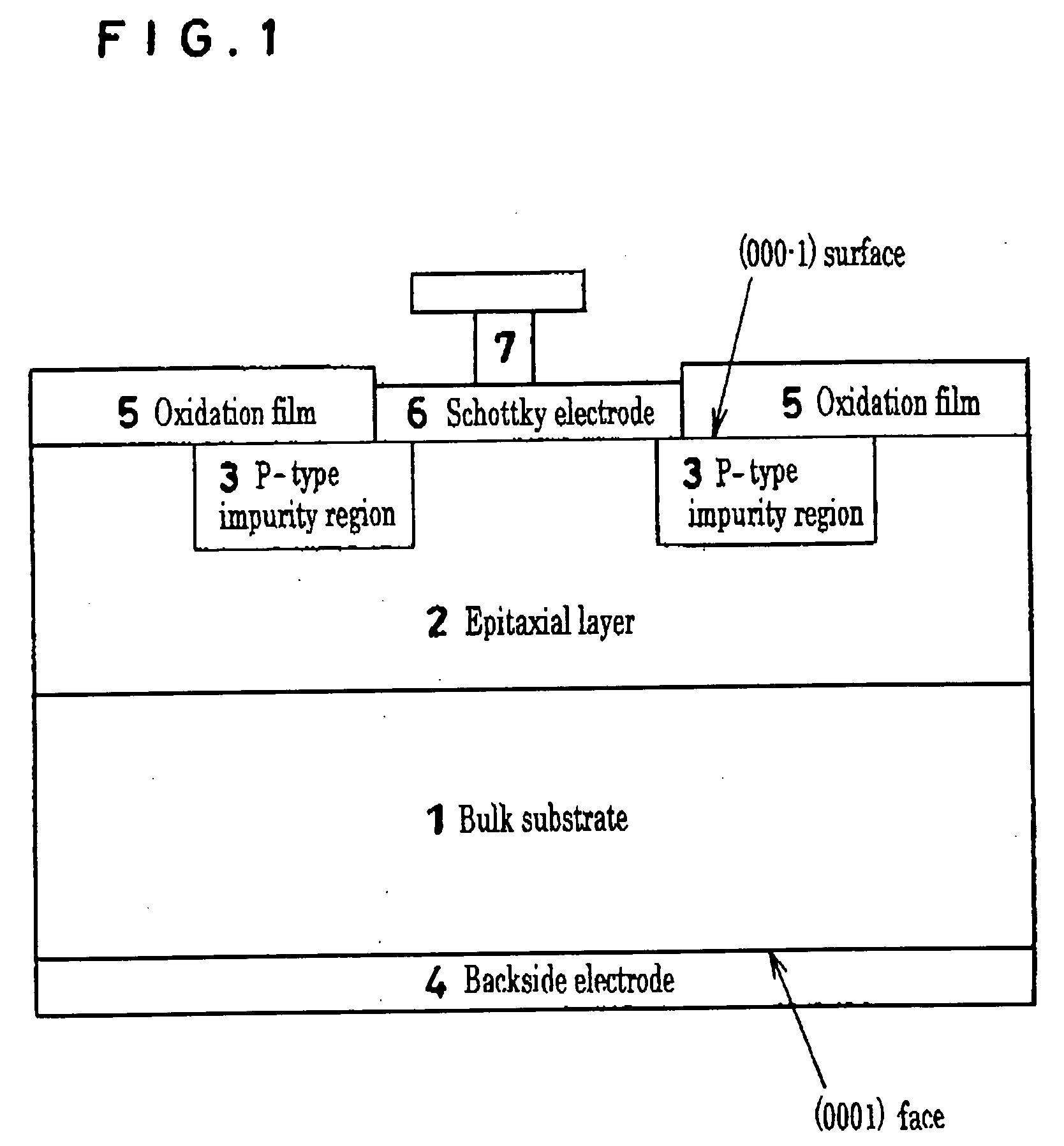
[0022]FIG. 1 is a cross-sectional schematic diagram of a Schottky barrier diode that is an example of the semiconductor device of the present invention.

[0023] This Schottky barrier diode was manufactured by the following procedure. First, the chemical vapor method was used to grow a 10 μm n type epitaxial layer 2 having a nitrogen impurity concentration of 1×...


PUM


Abstract

In a semiconductor device that uses a silicon carbide semiconductor substrate having p type, n type impurity semiconductor regions formed by ion implantation, the electrical characteristics of the end semiconductor device can be improved by decreasing the roughness of the silicon carbide semiconductor substrate surface. The semiconductor device of this invention is a Schottky barrier diode or a p-n type diode comprising at least one of a p type semiconductor region and n type semiconductor region selectively formed in a silicon carbide semiconductor region having an outermost surface layer surface that is a (000-1) surface or a surface inclined at an angle to the (000-1) surface, and a metal electrode formed on the outermost surface layer surface, that controls a direction in which electric current flows in a direction perpendicular to the outermost surface layer surface from application of a voltage to the metal electrode.

Description

TECHNICAL FIELD [0001] This invention relates to a semiconductor device formed on a silicon carbide substrate having a prescribed substrate crystalline surface orientation, and to an electric power converter, drive inverter, general-purpose inverter and super-power high-frequency communication equipment using the semiconductor device. BACKGROUND ART [0002] With respect to a semiconductor device using silicon carbide on the uppermost layer of a semiconductor substrate and to a method of manufacturing the same, as described in the following, there have been a number of publications and disclosures of inventions, but in the prior art, a semiconductor device using a silicon carbide substrate has a structure in which a gate electrode is normally formed on the (0001) face. In this case, when forming a p type or n type region by ion implantation in the (0001) face, ion implantation of a p type or n type impurity is followed by heat treatment at a high temperature of 1500° C. or above for a...

Claims


Application Information

Patent Timeline
Patent Type & Authority Applications(United States)
IPC IPC(8): H01L29/74H01L21/04H01L29/24H01L29/78H01L29/861H01L29/872
CPCH01L21/0445H01L29/1608H01L29/41766H01L29/7802H01L29/7838H01L29/861H01L29/872H01L21/18H01L29/04H01L29/7828
Inventor FUKUDA, KENJIKOSUGI, RYOJISENZAKI, JUNJIHARADA, SHINSUKE
Owner NAT INST OF ADVANCED IND SCI & TECH
Why Eureka
Try Eureka