Method of manufacturing semiconductor device having notched gate MOSFET

Inactive Publication Date: 2006-07-13
SAMSUNG ELECTRONICS CO LTD
View PDF13 Cites 13 Cited by
  • Summary
  • Abstract
  • Description
  • Claims
  • Application Information

AI Technical Summary

Benefits of technology

[0007] The present invention provides a method of manufacturing a semiconductor device, by which problems caused upon formation of a transistor having a reduced size required by a scaling technique for obtaining a su

Problems solved by technology

Hence, integrating the stacked SONOS transistor together with a logic product having a low initial threshold voltage Vth into a single chip is difficult due to the high initial threshold voltage Vth.
Also, in a stacked SONOS-type cell transistor, electrons trapped in a storage node layer within an ONO structure may move hor

Method used


Image

  • Method of manufacturing semiconductor device having notched gate MOSFET
  • Method of manufacturing semiconductor device having notched gate MOSFET
  • Method of manufacturing semiconductor device having notched gate MOSFET

Examples


Embodiment Construction

[0038] The present invention will now be described more fully with reference to the accompanying drawings, in which exemplary embodiments of the invention are shown. It should be noted that, throughout the description, unless noted otherwise, when a layer is described as being formed on another layer or on a substrate, the layer may be formed directly on the other layer or on the substrate, or one or more layers may be interposed between the layer and the other layer or the substrate.

[0039] This application incorporates by reference the entire contents of another U.S. Patent Application, filed on even date herewith, assigned to Samsung Electronics Co., Ltd., entitled, “Transistor Having Gate Dielectric Layer of Partial Thickness Difference and Method of Fabricating the Same,” naming as inventors Byung-yong Choi, Chang-woo Oh, Dong-gun Park and Dong-won Kim.

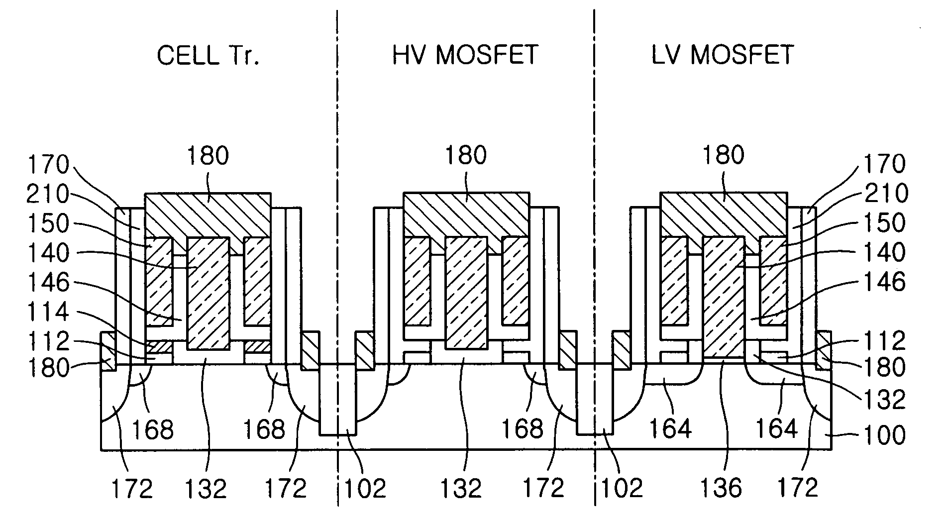
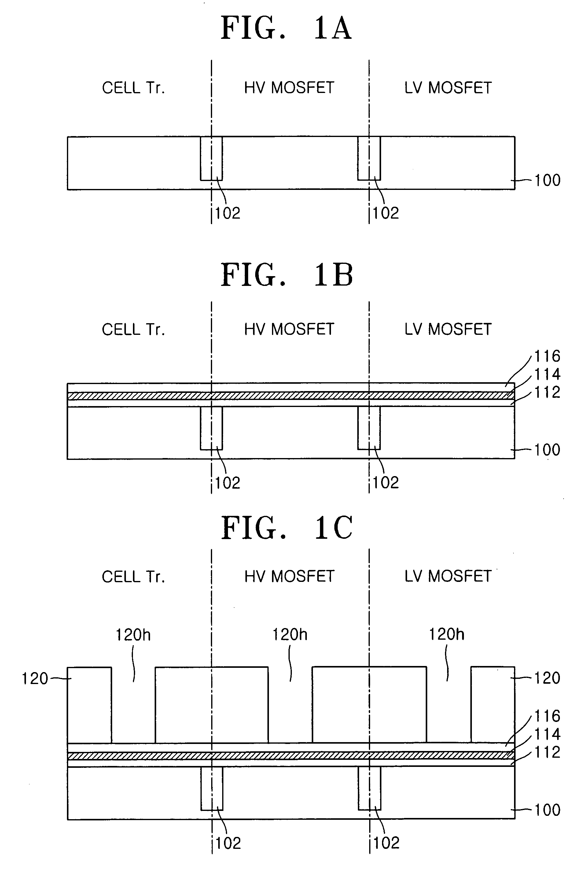
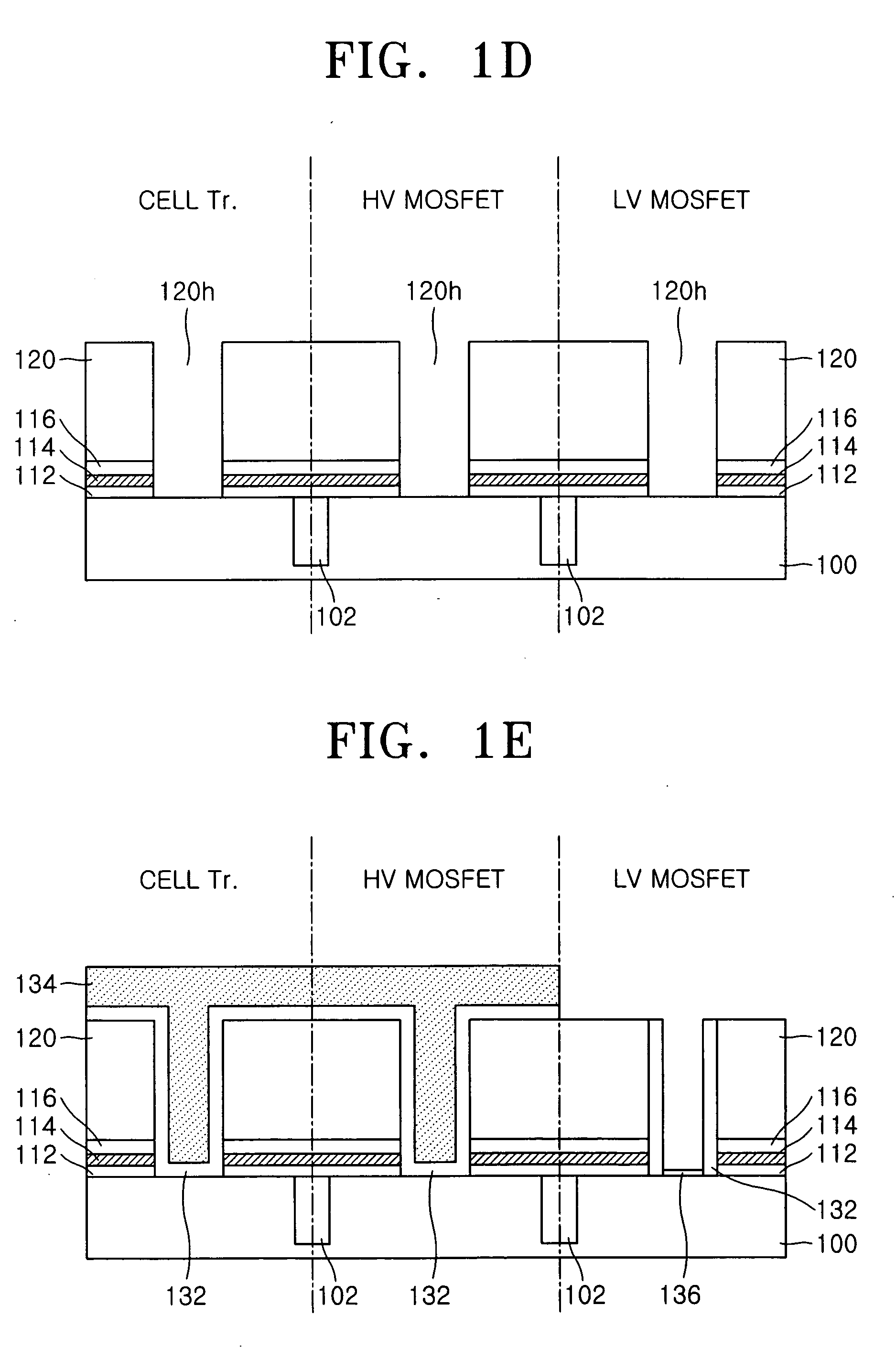
[0040]FIGS. 1A through 1O are cross-sectional views illustrating a method of manufacturing a semiconductor device according an...


PUM


Abstract

Provided is a method of manufacturing a semiconductor device, by which a cell transistor formed .on a cell array area of a semiconductor substrate employs a structure in which an electrode in the shape of spacers is used to form a gate and a multi-bit operation is possible using localized bits, and transistors having structures optimized to satisfy different requirements depending upon functions of the transistors can be formed on a peripheral circuit area which is the residual area of the semiconductor substrate. In this method, a cell transistor is formed on the cell array area. The cell transistor includes a notch gate structure, a first channel region formed on a semiconductor substrate under the notch gate structure, a source region and a drain region formed on both sides of the first channel region, a first gate insulation film formed between the first channel region and the notch gate structure, and a memory layer locally formed on areas adjacent to the source and drain regions between the first channel region and the notch gate structure. At the same time that the cell transistor is formed, a plurality of peripheral circuit transistors including at least one transistor having a different structure from the cell transistor are formed on the peripheral circuit area.

Description

CROSS-REFERENCE TO RELATED PATENT APPLICATIONS [0001] This application claims the benefit of Korean Patent Application Nos. 10-2005-0002877 filed on 12 Jan. 2005 and 10-2005-0015372, filed on Feb. 24, 2005, in the Korean Intellectual-Property Office, the contents of which are incorporated herein in their entirety by reference. BACKGROUND OF THE INVENTION [0002] 1. Field of the Invention [0003] The present invention relates to a method of manufacturing a semiconductor device, and more particularly, to a method of manufacturing a semiconductor device, by which process integration of a transistor capable of a multi-bit operation on a cell array area and a metal oxide semiconductor field effect transistor (MOSFET) on a peripheral circuit area is facilitated simultaneously. [0004] 2. Description of the Related Art [0005] Silicon-oxide-nitride-oxide-silicon (SONOS) or metal-oxide-nitride-oxide-silicon (MONOS) devices have been proposed as non-volatile memory devices that are widely used i...

Claims


Application Information

Patent Timeline
IPC IPC(8): H01L21/336
CPCH01L21/26586H01L29/665H01L29/66537H01L29/66553H01L29/6656H01L29/6659H01L29/66621H01L29/7833H01L29/7834
Inventor CHOI, BYUNG-YONGLEE, CHOONG-HOKIM, DONG-WONPARK, DONG-GUN
Owner SAMSUNG ELECTRONICS CO LTD
Why Eureka
Try Eureka