Semiconductor integrated circuit

a technology of integrated circuits and semiconductors, applied in the direction of digital storage, generating/distributing signals, pulse automatic control, etc., can solve the problems of unavoidable variations in channel width or the like, shortening the delay time, and worsening the input/output characteristics of the input/output characteristics, so as to achieve efficient utilization of time

Inactive Publication Date: 2006-07-20
PANASONIC SEMICON SOLUTIONS CO LTD
View PDF13 Cites 6 Cited by
  • Summary
  • Abstract
  • Description
  • Claims
  • Application Information

AI Technical Summary

Benefits of technology

[0013] It is an object of the present invention to make it possible to efficiently utilize the time before a clock generation circuit supplies a system clock signal, and in particular the time until the oscillation of a PLL circuit has stabilized.
[0015] More specifically, the reference clock signal is supplied to both a comparison clock input portion and a feedback clock input portion of the phase comparator while a feedback loop of the PLL circuit is interrupted, and the delay of a reset signal within the phase comparator is adjusted so as to reduce a detection dead zone of phase differences in the phase comparator.

Problems solved by technology

However in practice, there are cases in which it is not possible to detect tiny phase differences, so that there may be a dead zone of phase differences, and there may be discontinuities when the sensitivity is too high.
However, in the phase comparator according to a first piece of conventional technology, the delay time becomes shorter than the appropriate value because the reset circuit is made of one 4-input NAND circuit, and the input / output characteristics exhibit a dead zone (U.S. Pat. No. 3,610,954).
In the case of the second conventional technology, a worsening of the yield due to variations in the channel width or the like has become unavoidable with the sub-micron gate widths of recent transistors.
Charge pump circuits also have an aspect that worsens their input / output characteristics.
This means that even though clocks of the same phase are input, the phase difference is detected erroneously and a highly accurate PLL circuit cannot be realized.
Furthermore, clock drivers are designed such that they can supply a clock synchronized with zero skew to the function blocks, but due to temperature dependencies, process variations and the like, there are skew variations among chips.
Also, inside the function blocks, circuits that use two phases of clocks with clock synchronization, such as dynamic circuits or memories, are designed such that they can operate stably with some delay so as to avoid signal racing, but due to process variations, the margin between the two phases of the clocks may disappear, resulting in faulty operation.
Furthermore, there are function blocks that include the function of interrupting a series of operations when processing has become unnecessary during that series of operations, in order to reduce energy consumption, but depending on the operation frequency and process variations, the operation may not be halted completely, resulting in faulty operation.
Moreover, providing a tuning circuit in order to solve these problems is a waste of time, because the start of the operation of the tuning circuit needs to wait until the PLL circuit has stabilized.

Method used


Image

  • Semiconductor integrated circuit
  • Semiconductor integrated circuit
  • Semiconductor integrated circuit

Examples


embodiment 1

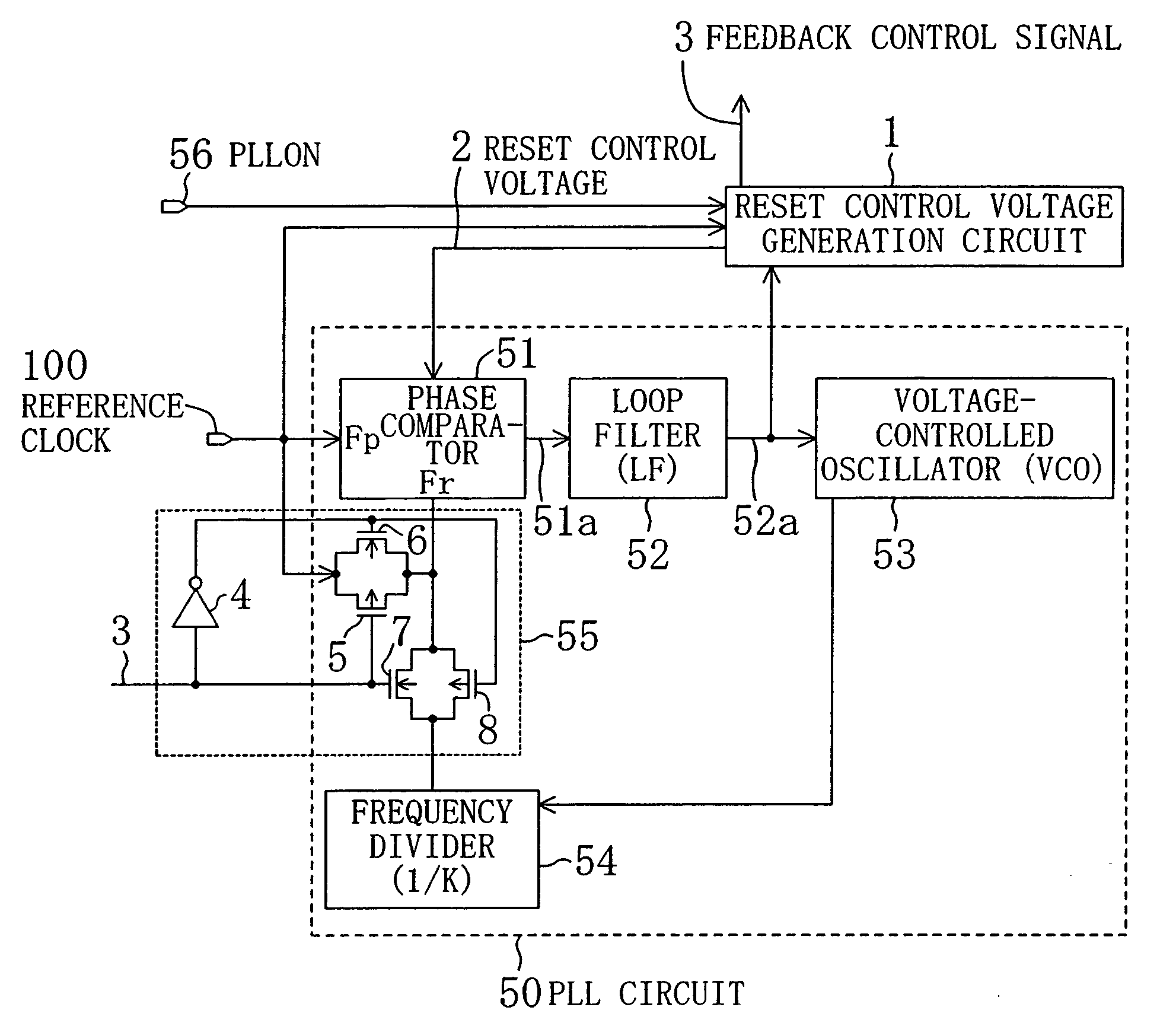
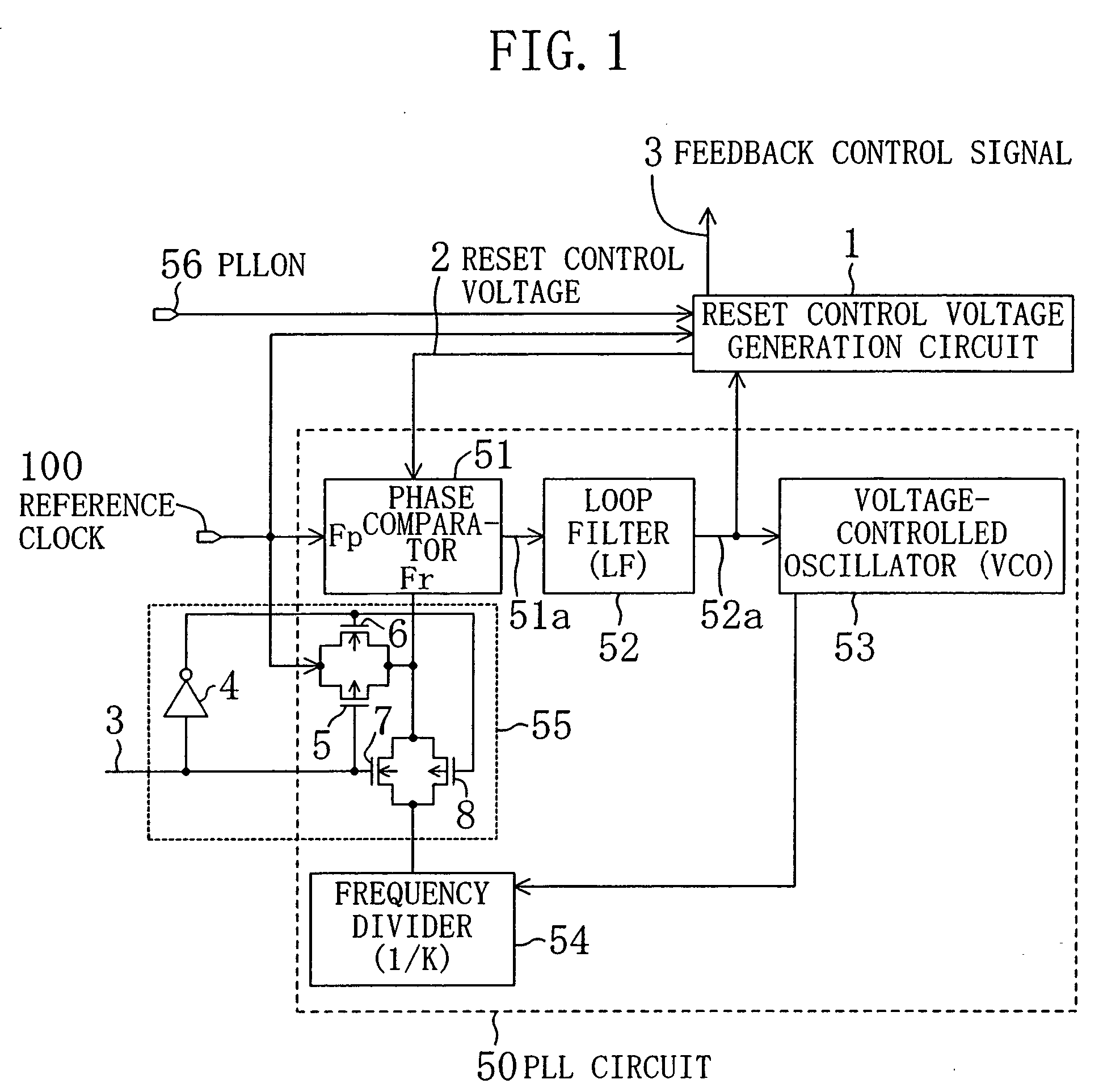
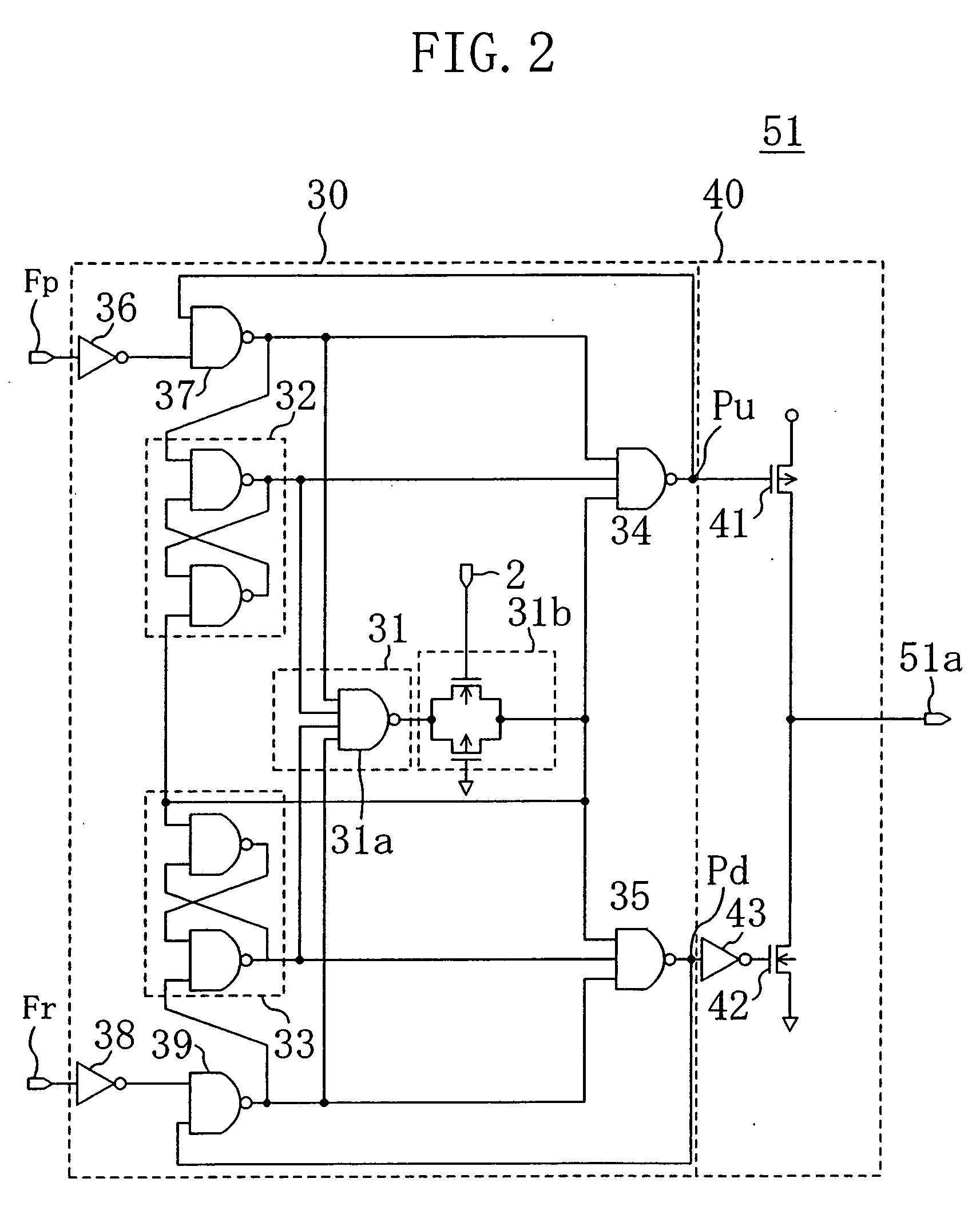
[0057]FIG. 1 is an example of a semiconductor integrated circuit according to the present invention, and is a block diagram illustrating a configuration example of a semiconductor integrated circuit incorporating a PLL circuit. In FIG. 1, numeral 50 denotes a PLL circuit including a phase comparator 51, a loop filter 52, a voltage-controlled oscillator 53, and a programmable frequency divider 54. The phase comparator 51 has input ports Fp and Fr, and compares the phases of the signals that are input into those two ports. A reference clock 100 is input into Fp. The output 51a of the phase comparator 51 is connected to the loop filter 52, the output 52a of the loop filter 52 is connected to the voltage-controlled oscillator 53, and the voltage-controlled oscillator 53 converts this input voltage into a frequency. The clock signal output from the voltage-controlled oscillator 53 is connected to the programmable frequency divider 54. The switch circuit 55 is controlled by a feedback con...

embodiment 2

[0070]FIG. 5 is another example of a semiconductor integrated circuit according to the present invention. The semiconductor integrated circuit in FIG. 5 has a PLL circuit 500 and a reference voltage circuit 600. The output of the charge pump circuit of the PLL circuit 500 is connected to a ripple detection circuit 900, and the output of the ripple detection circuit 900 is connected to a 2-bit incremental counter 910 that is incremented when ripples are detected. An output bus of this incremental counter 910 is connected to a control signal of switch circuits 930 that respectively connect En 626 to capacitors 920 and 921 when the control input e is “H,” and disconnect En 626 when the control input e is “L.” The capacitors 920 and 921 are respectively set to ¼ and ½ of the capacitance of a capacitor 630 inside the reference voltage circuit 600. The ripple detection circuit 900 is the circuit 210 explained for Embodiment 1, and also the incremental counter 910 is similar.

[0071]FIG. 6 ...

embodiment 3

[0077]FIG. 10 is an example of a semiconductor integrated circuit according to the present invention. The PLL circuit 800 in FIG. 10 is almost the same as the one in FIG. 6, and differs only with regard to the current charge pump circuit 801. The current charge pump circuit 801 in FIG. 10 is almost the same as the current charge pump circuit 520 in FIG. 6, but the drains of P-type MOS transistors 806 and 805 are connected to the point 804 connecting the P-type MOS transistors 807 and 802. The gate lengths of the P-type MOS transistors 806 and 805 are respectively two times and four times that of the P-type MOS transistor 807, and the various gates are controlled by bit signals 808 and 809 of a 2-bit register circuit output bus 840. The gates are connected to switch circuits 820 that are connected to Ep 651 when those bit signals are “H,” and to a power source when the bit signals are “L.” Furthermore, the drains of N-type MOS transistors 813 and 814 are connected to the point 810 co...


PUM


Abstract

During a period of preparation for actual operation, a reference clock is supplied to both a comparison clock input portion and a feedback clock input portion of a phase comparator while a feedback loop of a PLL (phase-locked loop) is interrupted, and a delay of a reset signal within the phase comparator is adjusted so as to reduce a detection dead zone of phase differences in the phase comparator.

Description

BACKGROUND OF THE INVENTION [0001] The present invention relates to semiconductor integrated circuits including a clock generation circuit, and more particularly to semiconductor integrated circuits in which a PLL (phase-locked loop) circuit is provided. [0002] Computing systems, such as microprocessors or microcontrollers, are provided with PLL circuits functioning as a clock multiplier circuit in order to realize the function of multiplying an external frequency at a portion of the central processing unit to perform high-speed operations. Furthermore, in recent microprocessors, it is desirable to be able to maintain the clock phase between an external bus and within the semiconductor integrated circuit with high precision. [0003] In conventional methods, the time that it takes until the PLL circuit stabilizes after the power has been turned on is counted with a timer, the clock supply from the PLL circuit to the central processing unit is halted for a certain amount of time, and t...

Claims


Application Information

Patent Timeline
Patent Type & Authority Applications(United States)
IPC IPC(8): H03L7/00G06F1/10G06F1/24G11C7/10H03D13/00H03L7/07H03L7/081H03L7/089H03L7/18
CPCG06F1/10G06F1/24G11C7/1072G11C7/222G11C7/227G11C2207/2281H03D13/004H03L7/07H03L7/0814H03L7/0891H03L7/0895H03L7/0898H03L7/18
Inventor SUMITA, MASAYA
Owner PANASONIC SEMICON SOLUTIONS CO LTD
Why Eureka
Try Eureka