
Memory device

a memory device and memory technology, applied in the field of memory, can solve the problems of low resistance state, deterioration of device characteristics, and sometimes destruction of stored data, and achieve the effect of improving retention characteristics

Inactive Publication Date: 2006-07-20
ELPIDA MEMORY INC
View PDF10 Cites 83 Cited by
  • Summary
  • Abstract
  • Description
  • Claims
  • Application Information

AI Technical Summary

Benefits of technology

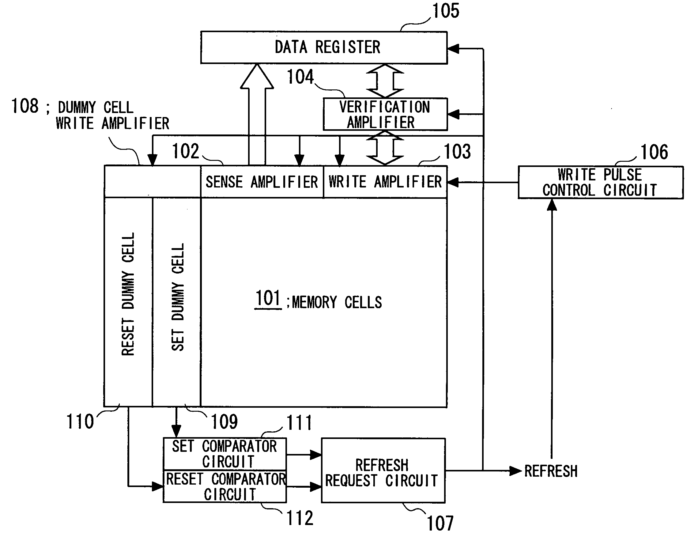
[0017] The fact that the phase change memory of the present invention is a DRAM interface compatible memory is exploited. There are provided reference cells stressed in accordance with the number of times of read and write operations. A change in the resistance value of the reference cells is detected and, if the resistance value have been changed beyond a predetermined reference value (specifically, to a low resistance value), a refresh request is issued to an internal circuit, not shown, to refresh a memory cell and a reference cell transitorily. In this manner, correction is made for variations in the programmed resistance value of the phase change device to assure the margin as well as to improve retention characteristic.
[0045] According to the present invention, it is possible to correct variations in the programmed resistance value of the phase change devices to provide the margin as well as to improve retention characteristic.

Problems solved by technology

There are occasions where device characteristics are deteriorated with repetition of read and write operations, with the result that stored data are sometimes destroyed (see FIG. 9 described hereinabove).
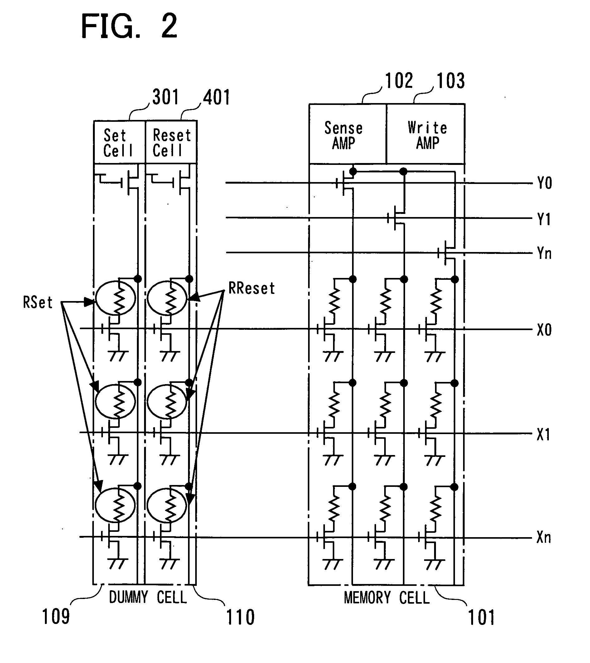
2) In case the same data are repeatedly written in the same cell, such a problem may arise that the low resistance state becomes more deeply low, such that, even though the write operation has been made to a state of a high resistance, the high resistance state is not completely established (see FIG. 9). FIG. 10 shows change and the distribution of the resistance value of a conventional phase change device on write and read, and specifically shows initial reset resistance distribution (RReset), reset resistance distribution after n times of the write operations (Rreset′), initial set resistance distribution (RSset) and set resistance distribution after n times of the write operations (Rset′).
In overwriting data, there is a possibility that status change is produced due to characteristics of a device of interest, and the resistance value is changed, with the result that resistance variations across the memory cells are increased, thus severely affecting the characteristics (see FIGS. 9 and 10).
If read / write is simply repeated, the result is deteriorated retention characteristic, due to characteristics of the phase change device, such that the functions of a memory device cannot be demonstrated.

Method used


Image

  • Memory device
  • Memory device
  • Memory device

Examples


Embodiment Construction

[0061] Preferred embodiments of the present invention will now be described. The memory device according to a mode for practicing the present invention includes a reference cell, stressed in accordance with the number of times of the phase change memory cell, and means for detecting a change in the resistance value of the phase change devices constituting the reference cell and issuing a refresh request to an internal circuit in case the resistance value has been changed beyond the set reference value (specifically, to a low resistance value), thereby improving data retention characteristic.

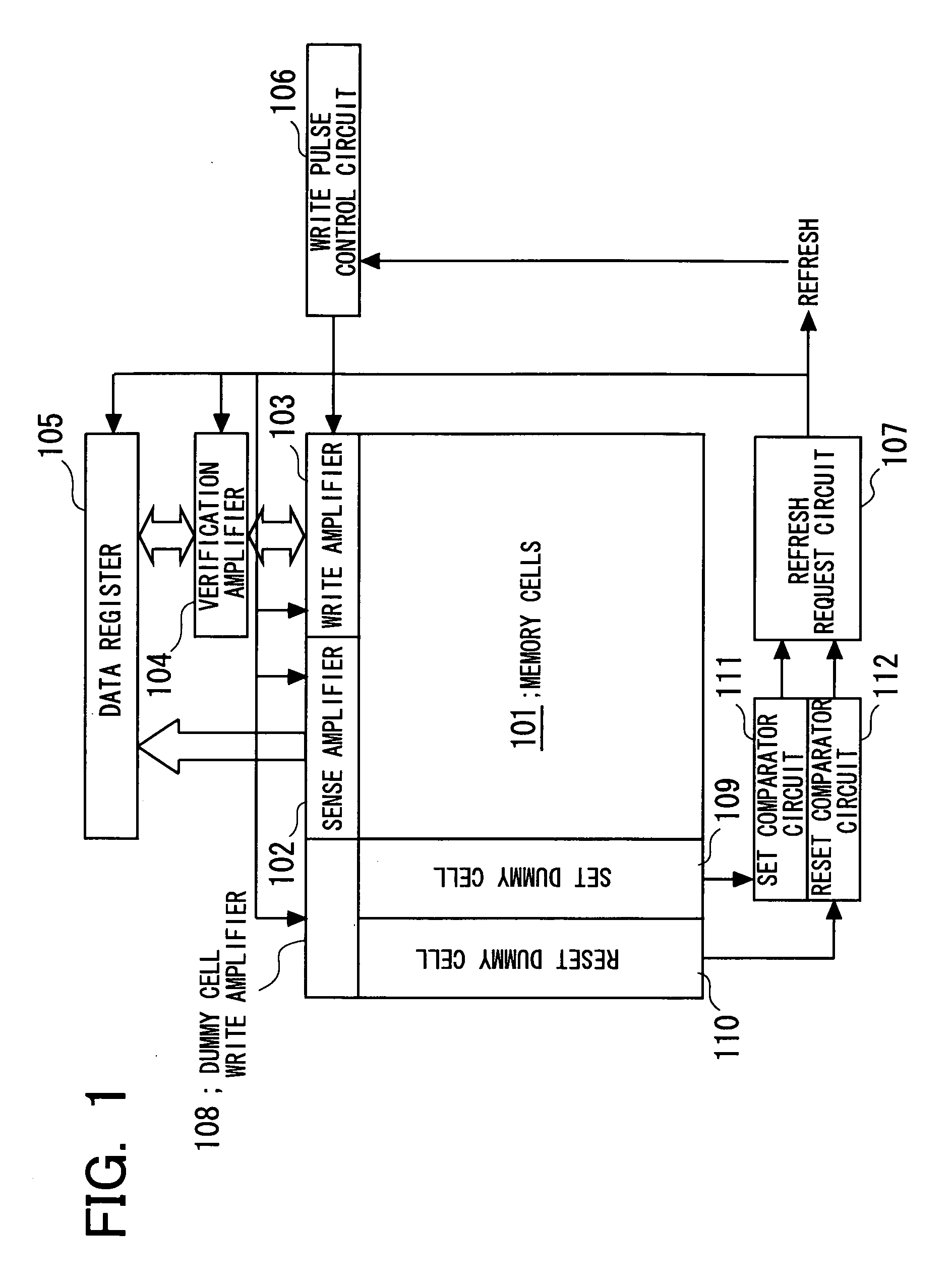
[0062] Preferred embodiments of the present invention will be described with reference to the drawings. Referring to FIG. 1, a memory according to an embodiment of the present invention includes a memory cell 101, a sense amplifier 102 for sensing and amplifying data written in the memory cell 101, a write amplifier 103 for writing data in the memory cell 101, a data register 105 for retreating ...


PUM


Abstract

Disclosed are a phase change memory with improved retention characteristic of a phase change device, and a method for refreshing the phase change memory. The fact that a memory is a DRAM interface compatible memory is exploited. There are provided dummy cells stressed in accordance with the number of times of read and write operations. Changes in the resistance value of the dummy cells are detected by comparator circuits. If the resistance value have been changed beyond a predetermined reference value (that is, changed to a low resistance), a refresh request circuit requests an internal circuit, not shown, to effect refreshing. The memory cells and the dummy cells are transitorily refreshed and correction is made for variations in the programmed resistance value of the phase change devices to assure the margin as well as to improve retention characteristic.

Description

FIELD OF THE INVENTION [0001] This invention relates to a memory with a programmable resistor element (phase change memory). BACKGROUND OF THE INVENTION [0002] A phase change memory, as typical of a memory with a programmable resistor element, is a non-volatile memory taking advantage of characteristics e.g. of a chalcogenide material, such as Ge, Sb or Te that, when the chalcogenide material is heated, it takes on an amorphous state (high resistance) / crystalline state (low resistance). In general, the material undergoes a transition between the high resistance (reset) state and the low resistance (set) state, by the Joule's heat, generated by the electric current, depending on the time duration of current application. [0003] In a phase change memory, the write time on the order of tens to about one hundred nanoseconds is said to be necessary. The number of times of repeated write operations is on the order of 1012, which is of the same order of magnitude as that of the FLASH memory...

Claims


Application Information

Patent Timeline
IPC IPC(8): G11C7/00
CPCG11C11/406G11C11/4099G11C11/5678G11C13/0004G11C13/0033G11C13/0064G11C13/0069G11C16/3431G11C16/349G11C2211/4061
Inventor FUJI, YUKIO
Owner ELPIDA MEMORY INC
Learn More