

Optical recording medium and process for producing the same, method for recording data on optical recording medium and method for reproducing data from optical recording medium
a technology of optical recording medium and optical recording medium, which is applied in the field of optical recording medium, can solve the problems of increasing the amount of laser energy absorbed by the secular deterioration of the optical transmitting layer will become greater, and the difficulty of forming various functional layers, etc., and achieves the effect of reducing the cost of developing and manufacturing a recording/reproducing devi
- Summary
- Abstract
- Description
- Claims
- Application Information
AI Technical Summary
Benefits of technology
Problems solved by technology
Method used
Image

Examples
examples
[0093] Examples of the present invention will be described hereunder. However, the present invention is not limited to the examples.
Manufacture of Samples
first example
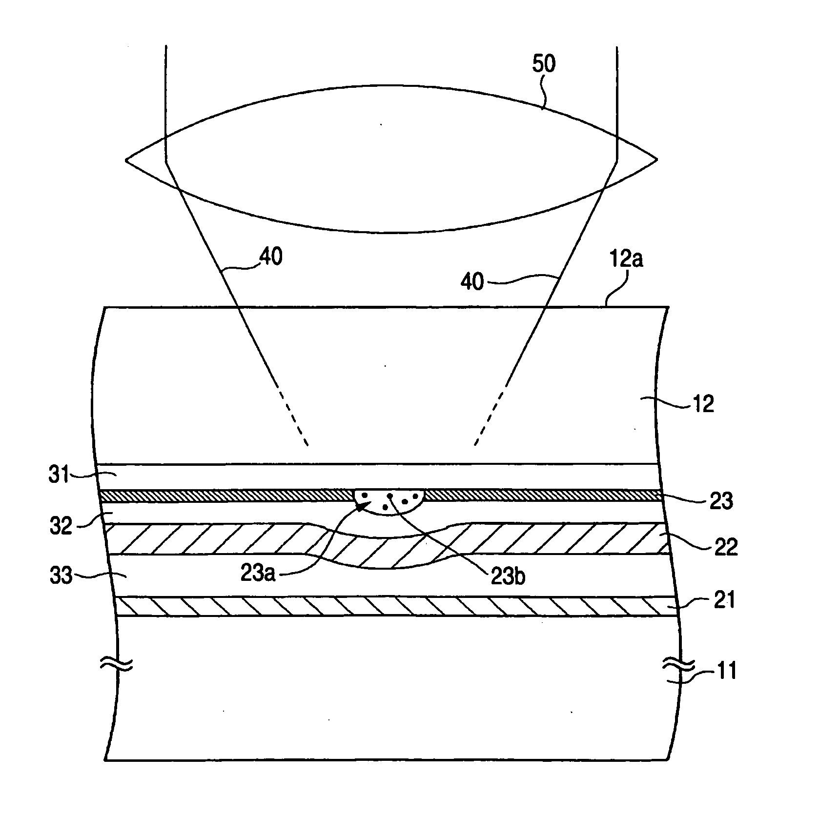
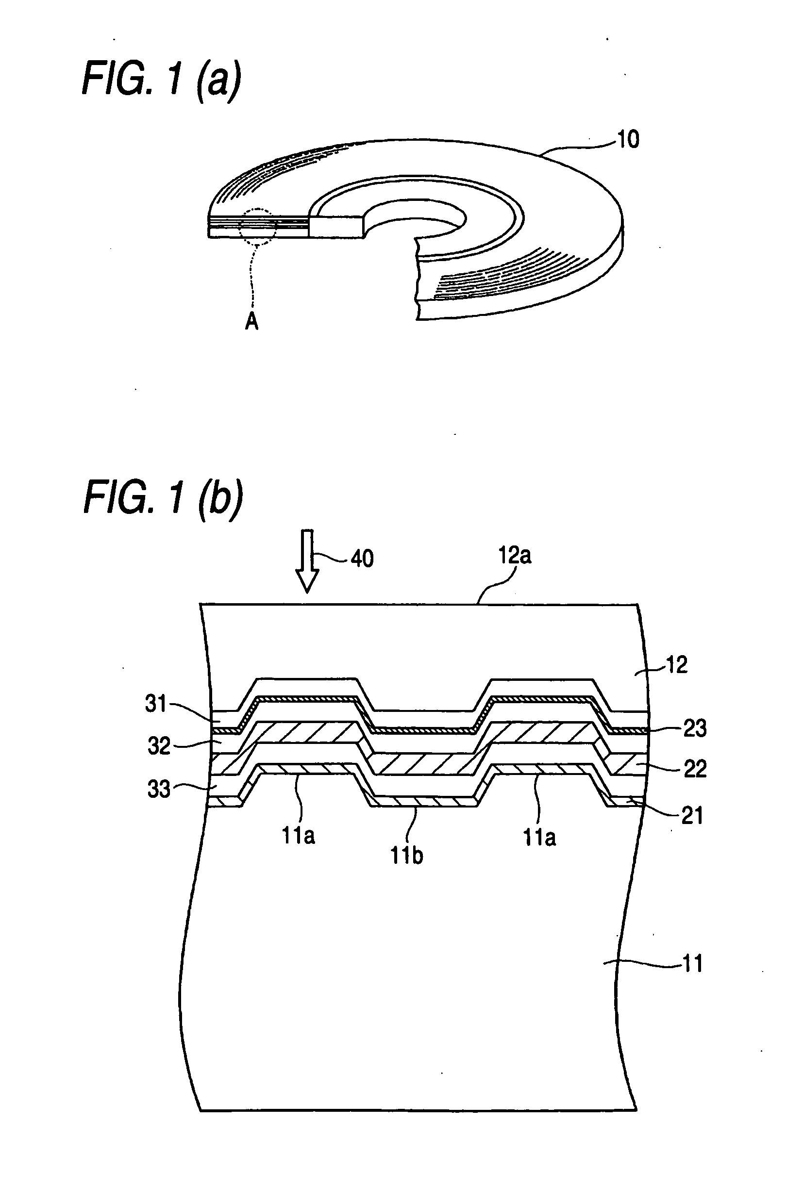
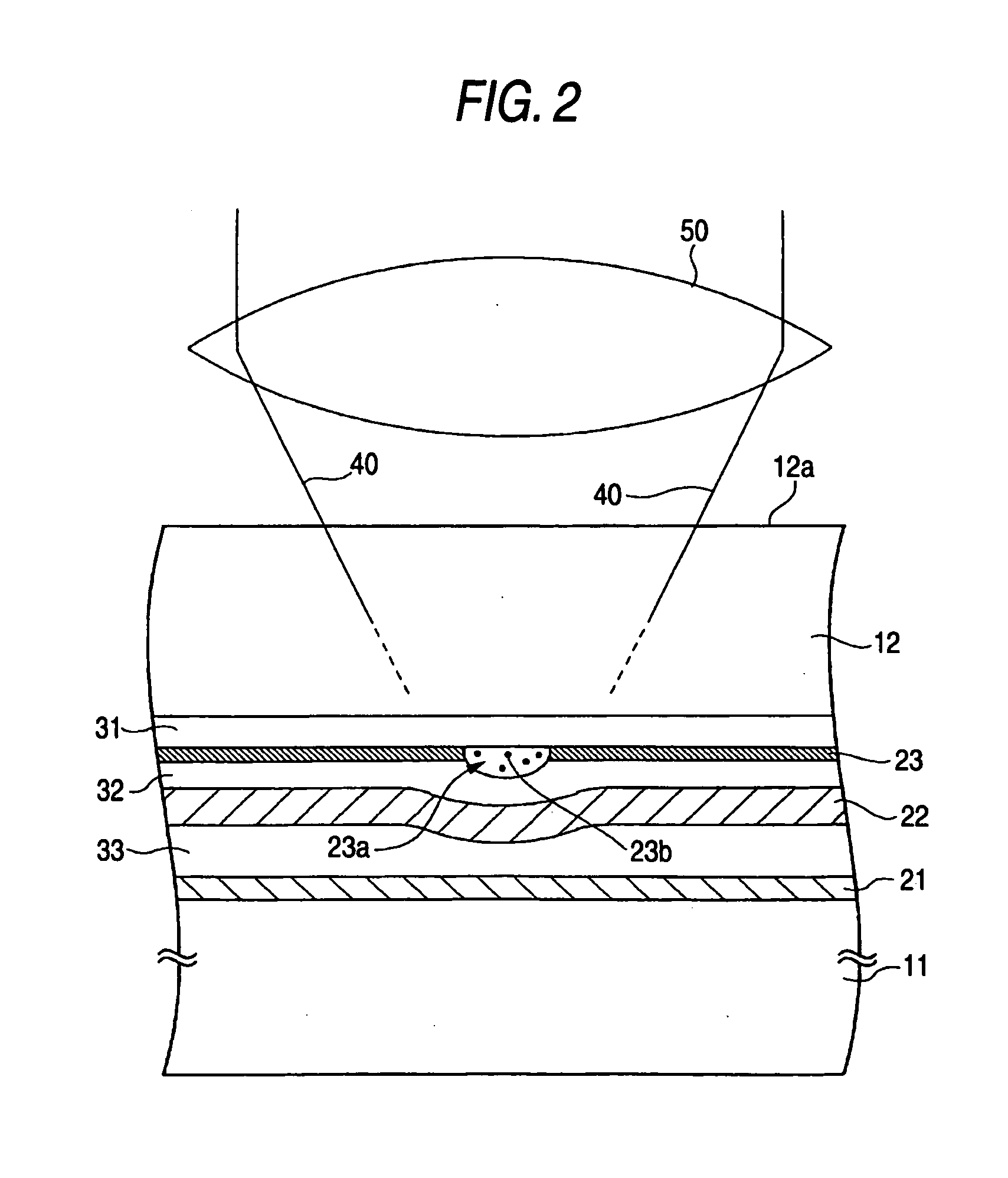
[0094] An optical recording medium sample having the same structure as that of the optical recording medium 10 shown in FIG. 1 was manufactured by the following method.
[0095] First, the disc-shaped support substrate 11, which has a thickness of about 1.1 mm, a diameter of about 120 mm, and the grooves 11a and the lands 11b formed in a front face of the substrate, was formed from polycarbonate by means of injection molding.
[0096] Next, the support substrate 11 was set in a sputtering system. In the side of the support substrate where the grooves 11a and the lands 11b are formed, there were sequentially formed the reflection layer 21 which is formed essentially from platinum (Pt) and has a thickness of about 20 nm; the dielectric layer 33 which is formed essentially from a mixture consisting of ZnS and SiO2 (a mol ratio of about 80:20) and has a thickness of about 100 nm; the light absorption layer 22 which is formed essentially from AgaInbSbcTed (a=5.9, b=4.4, c=61.1, d=28.6) and h...
second example
[0099] The reflection layer 21 was omitted. The thickness of the dielectric layer 33 was set to about 80 nm; the thickness of the dielectric layer 32 was set to about 40 nm; and the thickness of the dielectric layer 31 was set to about 100 nm. In other respects, an optical recording medium sample of a second example was produced in the same manner as was the optical recording medium of the first example.
PUM
| Property | Measurement | Unit |
|---|---|---|
| thickness | aaaaa | aaaaa |
| thickness | aaaaa | aaaaa |
| thickness | aaaaa | aaaaa |
Abstract
Description
Claims
Application Information