Plasma etching apparatus and plasma etching method

a technology of plasma etching and plasma etching, which is applied in the direction of electrical equipment, decorative arts, electric discharge tubes, etc., can solve the problems of in-plane non-uniformity of cd shift, and inability of plasma etching apparatus to ensure an adequate in-plane uniform etch rate over a wide area, and achieve high in-plane uniformity

Inactive Publication Date: 2006-08-03
HITACHI LTD +1
View PDF1 Cites 50 Cited by
  • Summary
  • Abstract
  • Description
  • Claims
  • Application Information

AI Technical Summary

Benefits of technology

[0026] As described above, according to the present invention, there are provided a plasma etching apparatus and a pla

Problems solved by technology

However, with the recent trend toward greater diameters of the process target object 1, the plasma etching apparatus has become unable to ensure an adequate in-plane uniformity of the etch rate over a wide area of the process target object 1 or an adequate in-plane uniformity of the gate width 8.
This may cause an in-plane nonuniformity of the CD shift.
Thus, a nonuniformity of the oxygen concentration may cause an in-plane nonuniformity of the CD shift.
In addition, if the in-plane uniformity of the etchant, such as radicals or ions of chlorine or bromine, in the vicinity of the surface of the process target object 1 is poor, the in-plane uniformity of the etch rate is also poor.
Thus, a poor in-plane uniformity of the etchant may cause an in-plane nonuniformity of the CD shift.
However, if the flow rate of the introduced process gas is too greatly increased, there is a possibility that the concentration of the reaction product in the central area of the process target object may be reduced excessively and may be lower than the concentration in the peripheral area.
Thus, there is a drawback that it is difficult to accomplish the etching process at a wide range of flow rates of the process gas.
However, the two process gases introduced to the central area of the process target object and to the circumference o

Method used


Image

  • Plasma etching apparatus and plasma etching method
  • Plasma etching apparatus and plasma etching method
  • Plasma etching apparatus and plasma etching method

Examples


Embodiment Construction

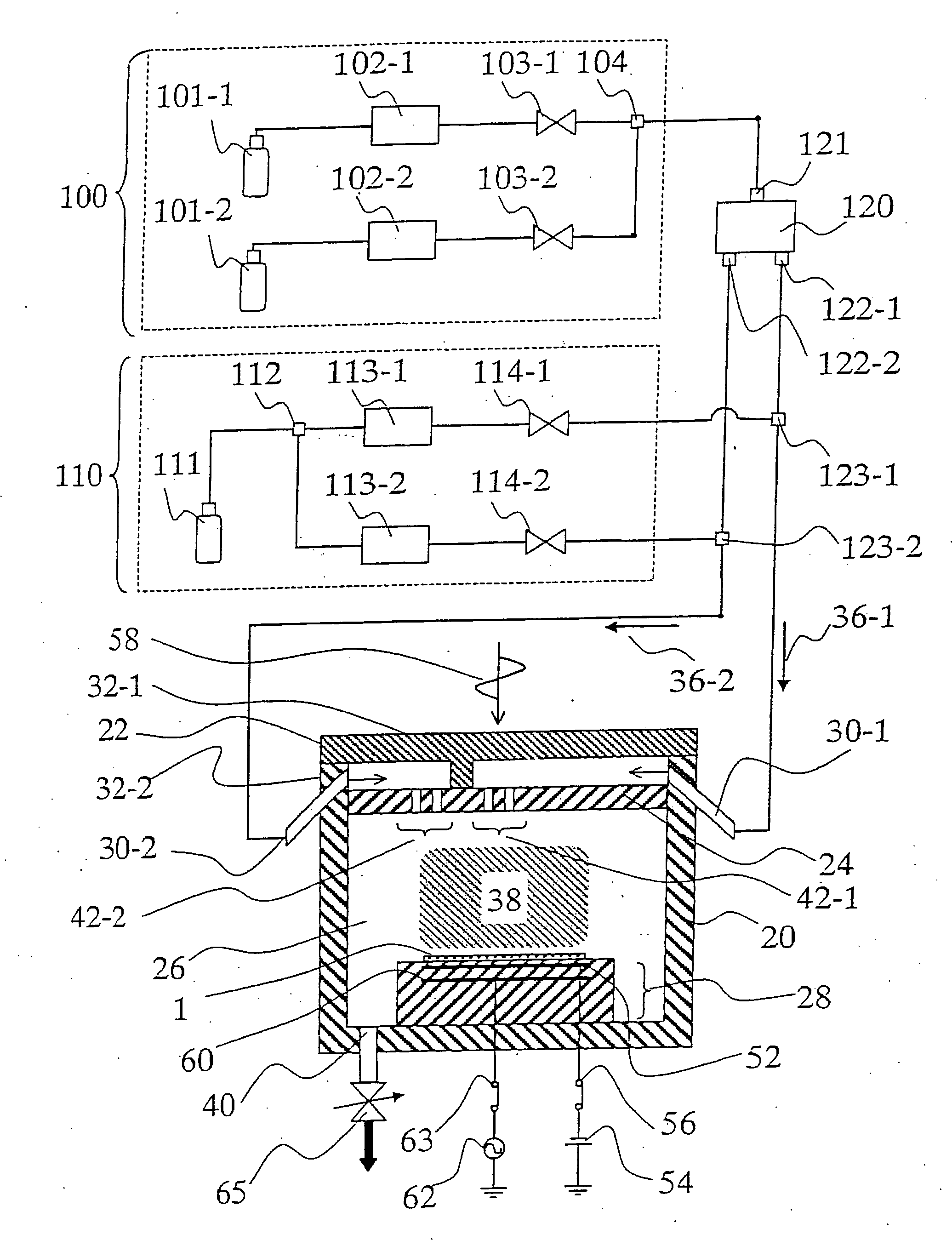
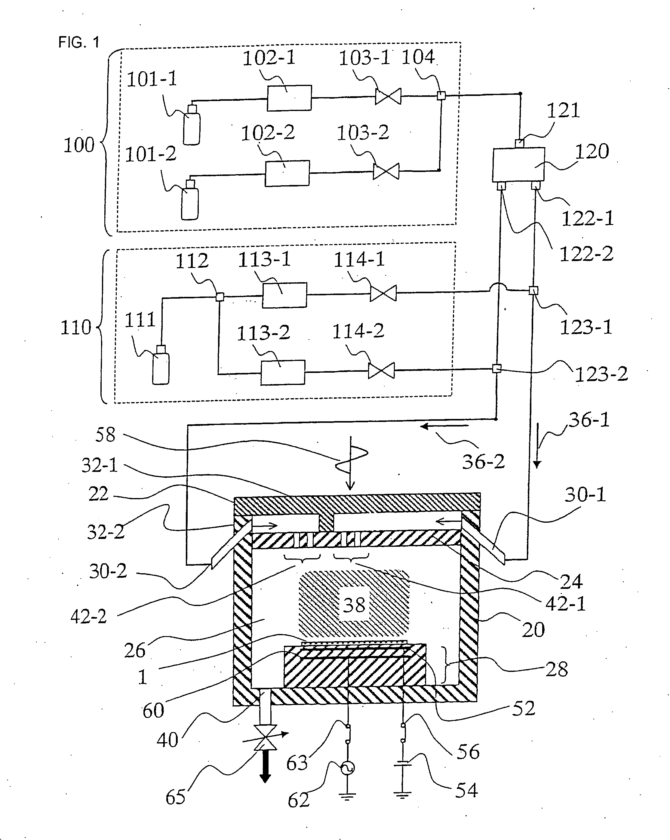
[0041] In the following, a first embodiment of the present invention will be described in detail with reference to FIGS. 1 to 5. First, with reference to FIG. 1, a microwave ECR plasma etching apparatus according to the first embodiment of the present invention and an arrangement of a gas system therefor will be described. According to the present invention, the gas supply system comprises a common gas subsystem (a first gas supply source) 100 and an additive gas subsystem (a second gas supply source) 110. The common gas subsystem 100 comprises gas supply means 101-1 and 101-2 as gas supply sources, flow controllers 102-1 and 102-2 for adjusting the flow rate of each gas, valves 103-1 and 103-2 for allowing or stopping the flow of each gas, and a confluence section 104 of the gasses in the common gas subsystem 100. In this embodiment, as common gasses, the gas supply means 101-1 supplies hydrogen bromide (HBr), and the gas supply means 101-2 supplies chlorine (Cl2).

[0042] The commo...


PUM

PropertyMeasurementUnit
Fractionaaaaaaaaaa
Fractionaaaaaaaaaa
Flow rateaaaaaaaaaa

Abstract

To provide a plasma etching apparatus that achieves a high in-plane uniformity of the CD shift.
A plasma etching apparatus includes: a process chamber 26 in which a plasma etching process is performed on a process target object 1;
A first gas supply source 100 for supplying a first process gas; a second gas supply source 110 for supplying a second process gas; a first gas introduction area 42-1 having a first gas introduction port for introducing the first process gas into the process chamber 26; a second gas introduction area 42-2 having a second gas introduction port 3 for introducing the second process gas into the process chamber 26; flow controllers 102, 113 for adjusting the flow rates of the process gasses; and a gas flow divider 120 for dividing the process gas into a plurality of gas flows, in which the first gas introduction port and the second gas introduction port are provided substantially in the same plane, and the first gas introduction area 42-1 and the second gas introduction area 42-2 are separated from each other.

Description

[0001] The present application is based on and claims priority of Japanese patent applications No. 2005-022113 filed on Jan. 28, 2005, the entire contents of which are hereby incorporated by reference. BACKGROUND OF THE INVENTION [0002] 1. Field of the Invention [0003] The present invention relates to a plasma etching apparatus that processes a semiconductor substrate, such as a semiconductor wafer, and a plasma etching method using the plasma etching apparatus. [0004] 2. Description of the Related Art [0005] Conventionally, in processes of manufacturing a semiconductor chip, a plasma etching apparatus using a reactive plasma is used to process a semiconductor substrate, such as a semiconductor wafer. [0006] Here, as an example of the plasma etching, an etching process for forming a polysilicon (poly-Si) gate electrode of a metal oxide semiconductor (MOS) transistor (referred to as a gate etching process, hereinafter) will be described with reference to FIG. 8. As shown in FIG. 8(a)...

Claims


Application Information

Patent Timeline
IPC IPC(8): C23F1/00H01L21/306
CPCH01J37/3244H01J37/32449H01L21/32137H01L21/67069
Inventor MIYA, GOTANAKA, JUNICHIKANNO, SEIICHIROMAKINO, AKITAKAYOSHIGAI, MOTOHIKO
Owner HITACHI LTD
Why Eureka
Try Eureka