Semiconductor device and manufacturing method thereof

a technology of semiconductors and thin films, applied in semiconductor lasers, solid-state devices, lasers, etc., can solve the problems of deteriorating device operation, heterogeneous materials, and high cost of materials for bulk substrates, and achieve the effect of sharp reduction of defect density and high quality

Inactive Publication Date: 2006-08-03
HITACHI LTD
View PDF14 Cites 142 Cited by
  • Summary
  • Abstract
  • Description
  • Claims
  • Application Information

AI Technical Summary

Benefits of technology

[0010] The present invention has been made in view of the above problems. Its purpose is to control precisely the production position and orientation of threading dislocations and defects by using an inexpensive substrate to provide a high quality semiconductor device whose defect density is sharply decreased and the manufacturing method thereof.

Problems solved by technology

These materials are very expensive for a bulk substrate, so that heterogeneous materials are used as a substrate in fabricating devices.
These lattice mismatches cause large strain between a substrate and a grown layer, producing a large number of defects such as threading dislocation and plane defect in the thin film, which markedly deteriorates device operation.
These defects lower a lifetime of a light emitting device and produce leak current in an electronic device.
The SiC substrate, however, is not suited industrially because it is expensive as compared to a sapphire or a Si substrate.
It is not enough to use a single effect produced by the above buffer layer or patterning for this purpose.
Even if a patterning effect is used, it is difficult to control precisely defects, and there still exist a large number of defects that do not disappear.
However, a plurality of defects concentrate in the same path, which makes a defect density very large at the meeting position of defects.

Method used


Image

  • Semiconductor device and manufacturing method thereof
  • Semiconductor device and manufacturing method thereof
  • Semiconductor device and manufacturing method thereof

Examples


first embodiment

[0050] Embodiments on a semiconductor device and the production method therefor related to the present invention are described in further detail with reference to accompanying drawings.

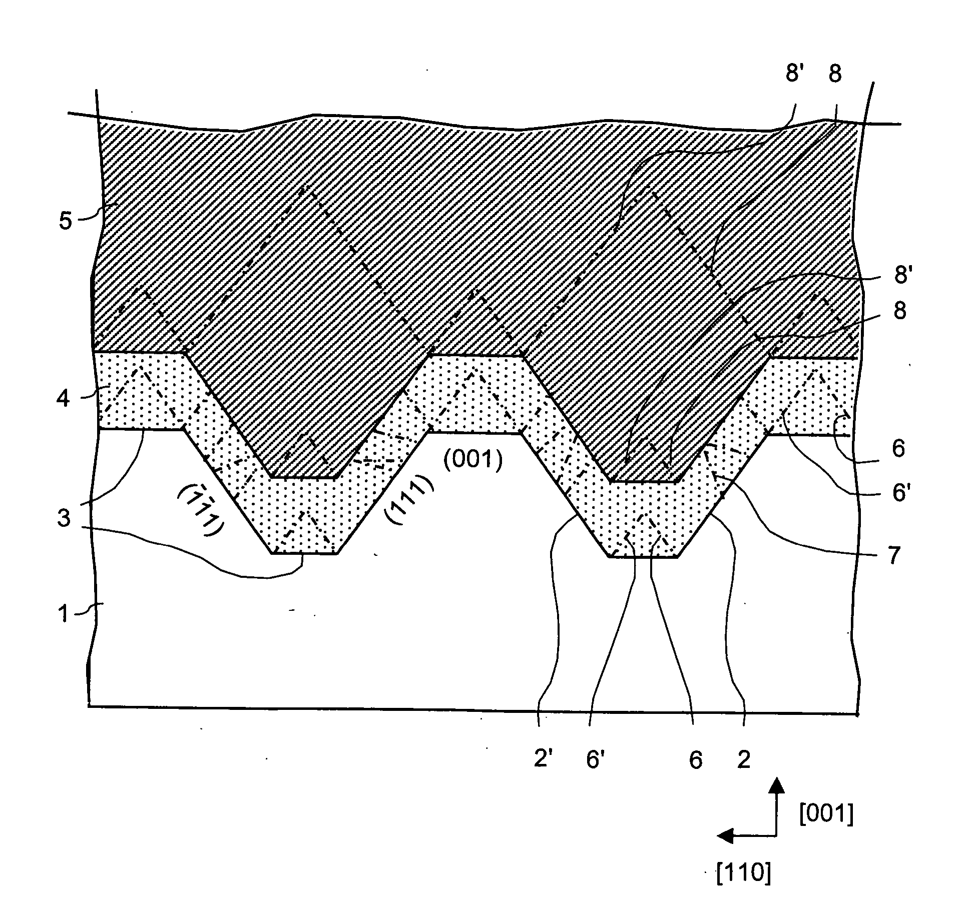
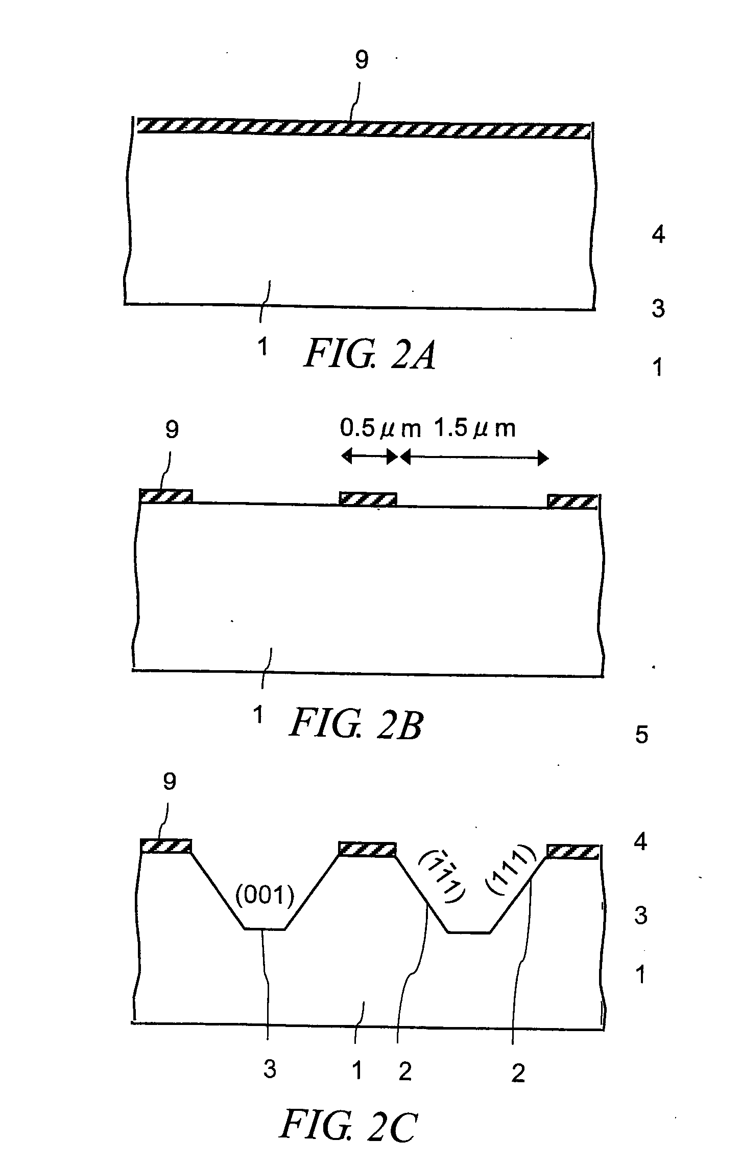
[0051]FIG. 1 a cross sectional view of a first embodiment of a semiconductor thin film related to the present invention. On a single crystal silicon (Si) substrate 1 are formed a plurality of pair of facets 2 and 2′ arranged in line. A threading dislocation density at the substrate surface where the facets are formed is less than 1 / cm2. At this point, the opposing facets 2 and 2′ have a form being mirror-symmetrical to an axis perpendicular to the substrate, i.e., to the surface orientation of the substrate. On the bottom of the grooves formed by the facets themselves and between the adjacent grooves lie flat portions 3. The flat portions do not always need to exist when the facets are formed, but it is preferable to form them in advance as shown in FIG. 1. An example without the flat portions is des...

second embodiment

[0057] The first embodiment describes spontaneous production of defects at an angle portion in forming SiC layer 5. Depending on growth conditions of SiC layer 5 and crystallinity of the buffer layer 4, it may be stable in energy to propagate defects in layer 4 into SiC layer 5 directly. In this situation, defects at angles are not produced in SiC layer 5, a large number of defects produced in the buffer layer 4 will propagate directly into the SiC layer 5. FIG. 7 is a cross sectional view of a semiconductor thin film showing a second embodiment related to the present invention in view of the above description. Here, the same reference characters as in the first embodiment are used, only differences from the first embodiment are extracted to describe. This embodiment is characterized in that the growth rate of (001) and (111) planes is regulated when the buffer layer 4 is grown so that defects 6 and 6′ can be always positioned at angles on the bottom of the groove on the surface of ...

third embodiment

[0058]FIG. 8 is a cross sectional view of a semiconductor thin film shown in a third embodiment related to the present invention. Description will be made also using the same reference characters as in the first embodiment. In the present embodiment double SiGeC layers 4a and 4b different from each other in Ge composition are used as semiconductor buffer layer 4. Layer 4a right on substrate 1 is characterized by containing more Ge than layer 4b in composition. It is supposed that both the first and the second SiGeC layer 4a and 4b share defects 6a and 6a′ and 6b and 6b′ produced from angles made by facets and flat portions. Even in the present embodiment, the first SiGeC layer with more Ge—C bonds acts as a buffer for the second SiGeC layer, and the second layer also acts as a buffer for SiC layer 5. This can gradually decrease defects, which will be effective if decrease in defect is not sufficient in the first buffer. In the present embodiment, double SiGeC buffer layers 4 are tak...


PUM

PropertyMeasurementUnit
temperaturesaaaaaaaaaa
thicknessaaaaaaaaaa
widthaaaaaaaaaa

Abstract

A high quality silicon carbide (SiC) layer being substantially lower in threading dislocation density than a prior layer is formed on silicon (Si) substrate. A semiconductor device is fabricated in such a way that a semiconductor buffer layer containing Si in part and being higher in defect density than a Si substrate is formed on the Si substrate on the upper portion of which are formed a plurality of pairs of facets being mirror-symmetrical to the surface orientation of a semiconductor substrate, further on the top of the layer a SiC layer is sequentially formed.

Description

CROSS-REFERENCE TO RELATED APPLICATION [0001] The present application claims priority from Japanese Patent Application No. JP 2005-5841 filed on Jan. 13, 2005, the content of which is hereby incorporated by reference into this application. TECHNICAL FIELD OF THE INVENTION [0002] The present invention relates to a semiconductor thin film comprised of silicon carbide (SiC) formed on, for example, a silicon (Si) substrate, and a method of manufacturing thereof, and in particular, to a semiconductor device in which the SiC film is formed as a virtual substrate for an electronic and a light emitting device and to a method of manufacturing thereof. BACKGROUND OF THE INVENTION [0003] Wide energy band gap semiconductor materials such as a III-nitride semiconductor and silicon nitride (SiC) have had a wide range of applications to light emitting elements in blue-ultraviolet range and high-frequency high-output devices and have been growing in importance more and more in late years. These mat...

Claims


Application Information

Patent Timeline
Patent Type & Authority Applications(United States)
IPC IPC(8): H01L33/00H01S5/20H01L33/06H01L33/10H01L33/12H01L33/16H01L33/32H01L33/34H01L33/42
CPCH01L21/02381H01L21/0243H01L21/02433H01L21/02447H01L21/0245H01L21/02502H01L21/02505H01L21/02529H01L21/0262H01L33/12
Inventor MIURA, MAKOTOODA, KATSUYAWASHIO, KATSUYOSHI
Owner HITACHI LTD
Why Eureka
Try Eureka