Circuit board and semiconductor device

Active Publication Date: 2006-08-03
RENESAS ELECTRONICS CORP
View PDF6 Cites 23 Cited by
  • Summary
  • Abstract
  • Description
  • Claims
  • Application Information

AI Technical Summary

Benefits of technology

[0016] According to the semiconductor device or the circuit board of the present invention, increase in the space can b

Problems solved by technology

However, a high peaking amount making up for signal attenuation is required because the signal attenuation caused by the parasitic capacity in the circuits is increased when a required operating frequency is high.
Moreover, there has been further another probl

Method used


Image

  • Circuit board and semiconductor device
  • Circuit board and semiconductor device
  • Circuit board and semiconductor device

Examples


Example

First Embodiment

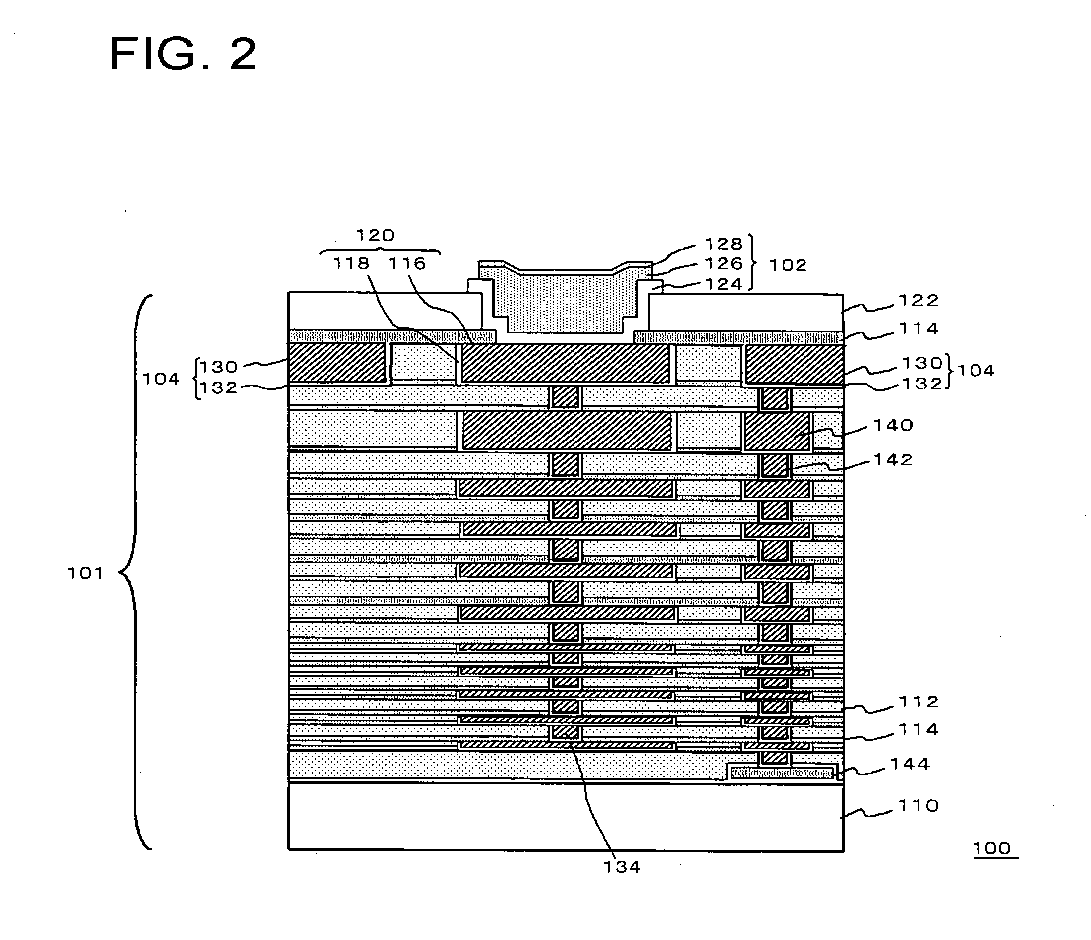
[0040] In the present embodiment, a circuit board is a semiconductor device. In the embodiment, a substrate includes a semiconductor substrate, and a multilayered interconnect structure formed thereon. Moreover, a terminal for flip-chip packaging (hereinafter referred to as a flip-chip packaging terminal as well) is a pad for flip-chip packaging (hereinafter referred to as a flip-chip packaging pad as well). A semiconductor device 100 according the embodiment may be configured to function as a differential amplification circuit shown in above-described drawing 14.

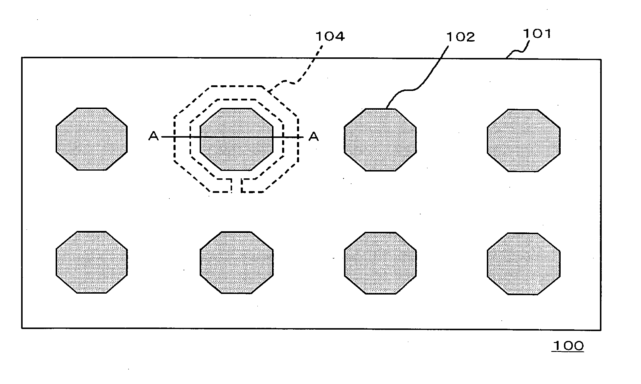
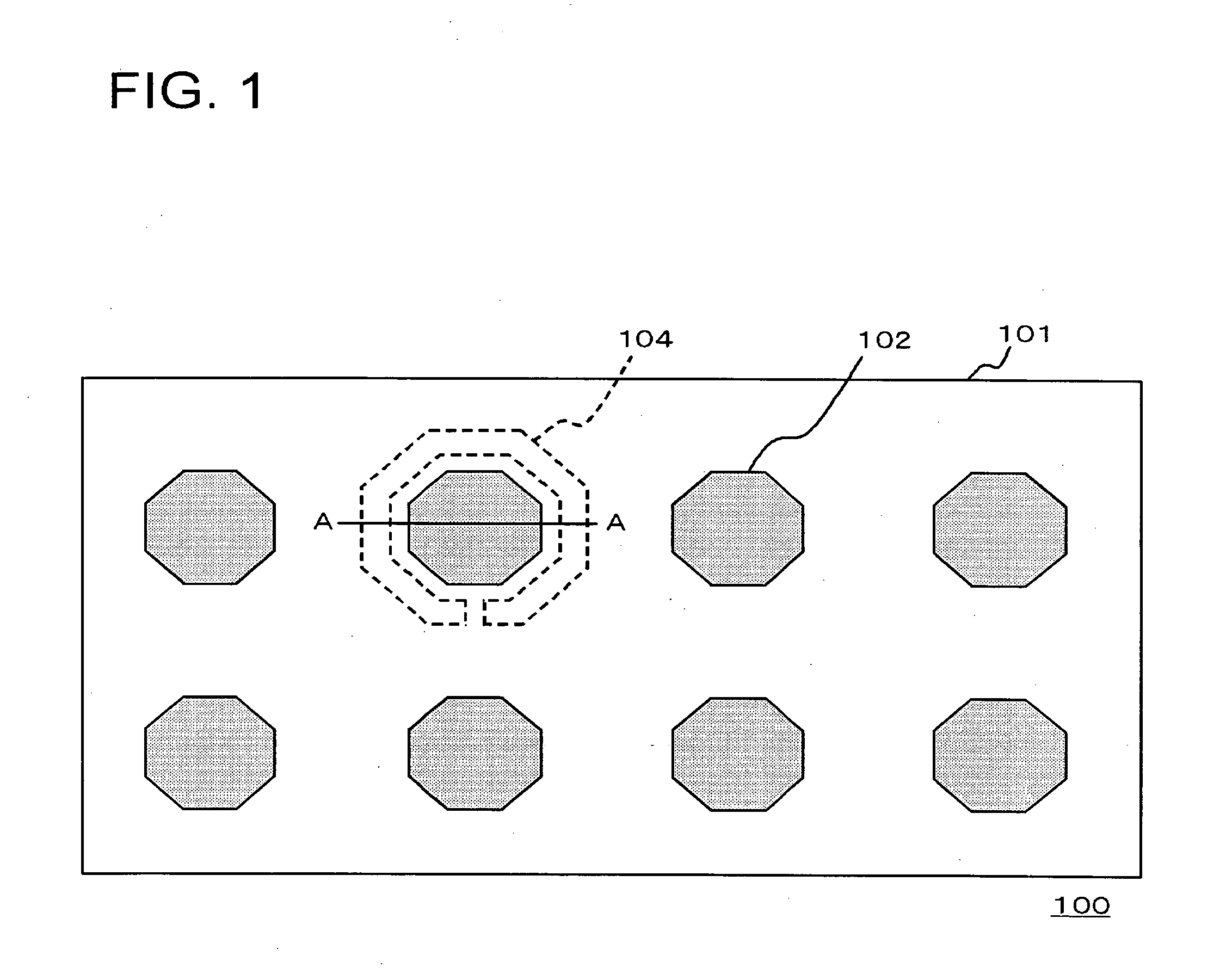
[0041]FIG. 1 is a top view showing a configuration of the semiconductor device according to the embodiment.

[0042] The semiconductor device 100 includes: a substrate 101; a plurality of flip-chip packaging pads 102 plane-arranged on the surface of the substrate 101; and a spiral inductor 104 formed so that the inductor 104 encloses one of the flip-chip packaging pads 102 in a plan view. Here, the plurality...

Example

Second Embodiment

[0060] In the present embodiment, a circuit board is a spacer having a plurality of through electrodes. In the embodiment, one end of the through electrode serves as a flip-chip packaging terminal.

[0061]FIG. 12A and FIG. 12B are views showing a configuration of the spacer according to the embodiment. FIG. 12A is a top view of the spacer, and FIG. 12B is a sectional view taken along the B-B line in FIG. 12A.

[0062] A spacer 200 includes: a substrate 201; a plurality of through electrodes 202a and 202b each of which has one end plane-arranged on the surface of the substrate 201; and a plurality of spiral inductors 204 which are formed so that each of the spiral inductors 204 encloses one of the plurality of through electrodes 202a. The substrate 201 may be, for example, a glass substrate, or a silicon substrate. In the embodiment, both ends of each spiral inductor 204 are connected to any one of the through electrodes 202b. However, the through electrode 202a enclos...


PUM


Abstract

A semiconductor device, includes: a semiconductor substrate; a multilayered interconnect structure formed on the semiconductor substrate; a terminal for flip-chip packaging arranged on the surface of the multilayered interconnect structure; and a spiral inductor formed to enclose the terminal for flip-chip packaging, in a plan view, which is not electrically connected with the spiral inductor. The spiral inductor may be provided for peaking by which the gain reduction caused in a high frequency is compensated.

Description

[0001] This application is based on Japanese Patent application NO. 2005-027298, the content of which is incorporated hereinto by reference. BACKGROUND [0002] 1. Technical Field [0003] The present invention relates to a circuit board, and a semiconductor device, which include an inductor. [0004] 2. Related Art [0005]FIG. 14 is a view showing a differential amplification circuit disclosed in Japanese Laid-open patent publication NO. 2004-274463. The differential amplification circuit includes: a current-controlled transistor 3; a single pair of active transistors 2a and 2b; a load resistances 1a and 1b; and load inductors 11a and 11b. The sources of active transistors 2a and 2b are connected to the drain of the current-controlled transistor 3, respectively. The load resistances 1a and 1b are connected to the drains of the active transistors 2a and 2b, respectively. One end of the load resistance 1a is connected to the load resistance 1a. One end of the load inductor 11b is connected ...

Claims


Application Information

Patent Timeline
IPC IPC(8): H01L29/00
CPCH01F17/0013H01L23/5227H01L24/13H01L24/10H01L2224/13099H01L2924/01013H01L2924/01029H01L2924/14H01L2924/1423H01L2924/19041H01L2924/19042H01L2924/19043H01L2924/30107H01L2924/3011H05K1/0233H05K1/111H05K1/165H05K2201/0792H05K2201/09809H05K2201/10674H01L2924/01005H01L2924/01006H01L2924/01033H01L2924/00H01L24/05H01L2224/05001H01L2224/05022H01L2224/05147H01L2224/05572H01L2224/056H01L2224/0615H01L2224/13H01L2924/15788Y02P70/50H01L2924/00014
Inventor NAKASHIBA, YASUTAKA
Owner RENESAS ELECTRONICS CORP
Why Eureka
Try Eureka