Method and apparatus to confine plasma and to enhance flow conductance

a technology of flow conductance and plasma, applied in the direction of adhesives, electrical discharge tubes, decorative arts, etc., can solve the problems of process drift, etching byproduct deposition in downstream areas, and reduce process throughput, so as to achieve the effect of enhancing flow conductan

Inactive Publication Date: 2006-08-03
APPLIED MATERIALS INC
View PDF15 Cites 26 Cited by
  • Summary
  • Abstract
  • Description
  • Claims
  • Application Information

AI Technical Summary

Benefits of technology

[0007] The embodiments of the present invention generally relate to a method and an apparatus to confine plasma and to enhance flow conductance in plasma processing reactors. In one embodiment, an apparatus configured to confine a plasma within a substrate processing region during processing a substrate in a plasma processing chamber comprises a substrate support having one or more dielectric layers, an annular ring surrounding the top portion of the substrate support, wherein there is a gap between the annular ring and process chamber walls having a gap width from about 0.8 inch to about 1.5 inch, and a dielectric seal placed between a top electrode and a process chamber body, wherein impedances of the top electrode, the dielectric seal, the substrate along with the substrate support, and plasma reduce a voltage supplied to the top electrode by a voltage ratio and supply the remaining voltage supplied to the top electrode at a negative phase at the substrate and the substrate support during plasma processing.

Problems solved by technology

Etch-byproduct deposition on the chamber walls could cause the process to drift.
In addition, unconfined plasmas could also cause etch-byproduct deposition in the downstream areas.
The accumulated etch-byproduct can flake off and result in particles.
To reduce the particle issues caused by the deposition of etch-byproduct in the downstream areas, additional downstream clean is needed, which could reduce process throughput and increase processing cost.
Plasma confinement devices, such as a slotted plasma confinement ring, could cause flow resistance for the gas flow to the downstream and results in pressure in the plasma chamber that is not low enough (e.g. ≦30 mTorr) for the FEOL applications described.

Method used


Image

  • Method and apparatus to confine plasma and to enhance flow conductance
  • Method and apparatus to confine plasma and to enhance flow conductance
  • Method and apparatus to confine plasma and to enhance flow conductance

Examples


Embodiment Construction

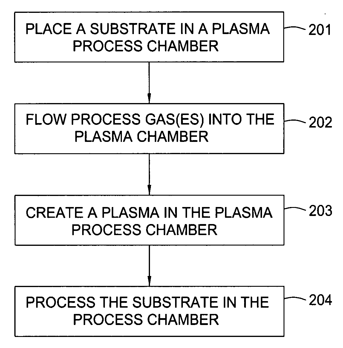
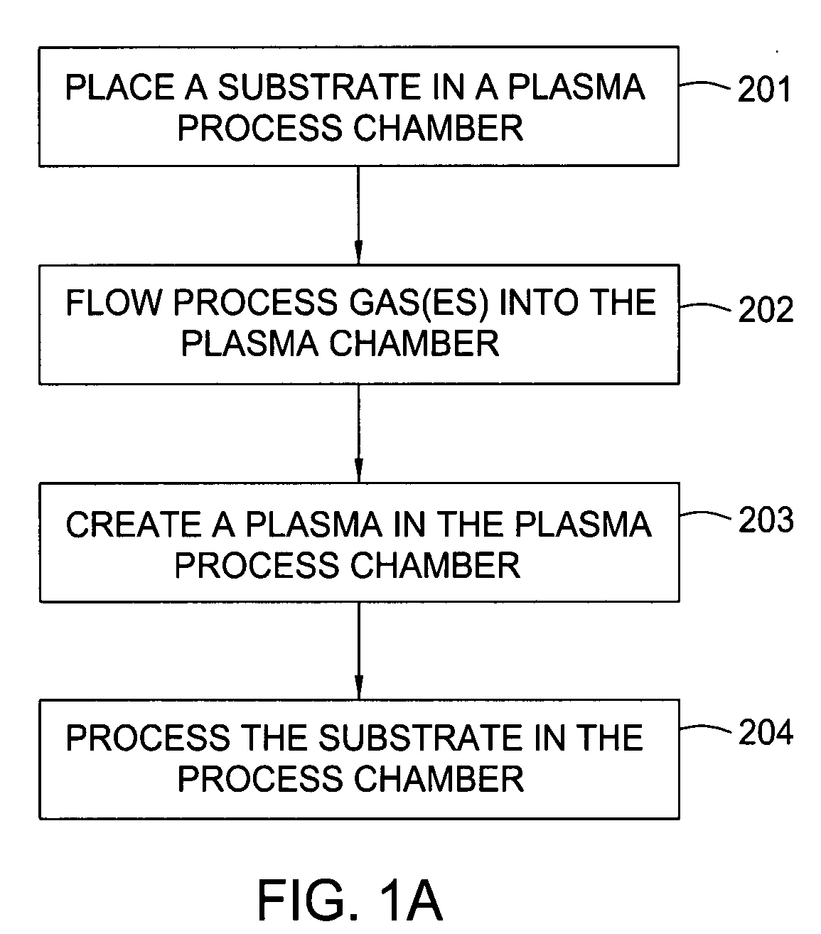
[0033] The process of processing a substrate in a plasma process chamber is shown in FIG. 1A. The process starts at step 201 by placing a substrate in a plasma process chamber. Next at step 202, process gas(es) is flown into the plasma process chamber. Then at step 203, a plasma is created in the plasma process chamber. At step 204, the substrate is processed in the plasma process chamber. The processing conducted in the plasma process chamber could be deposition, etching or plasma-treatment. The concept of the invention applies to any types of plasma processing.

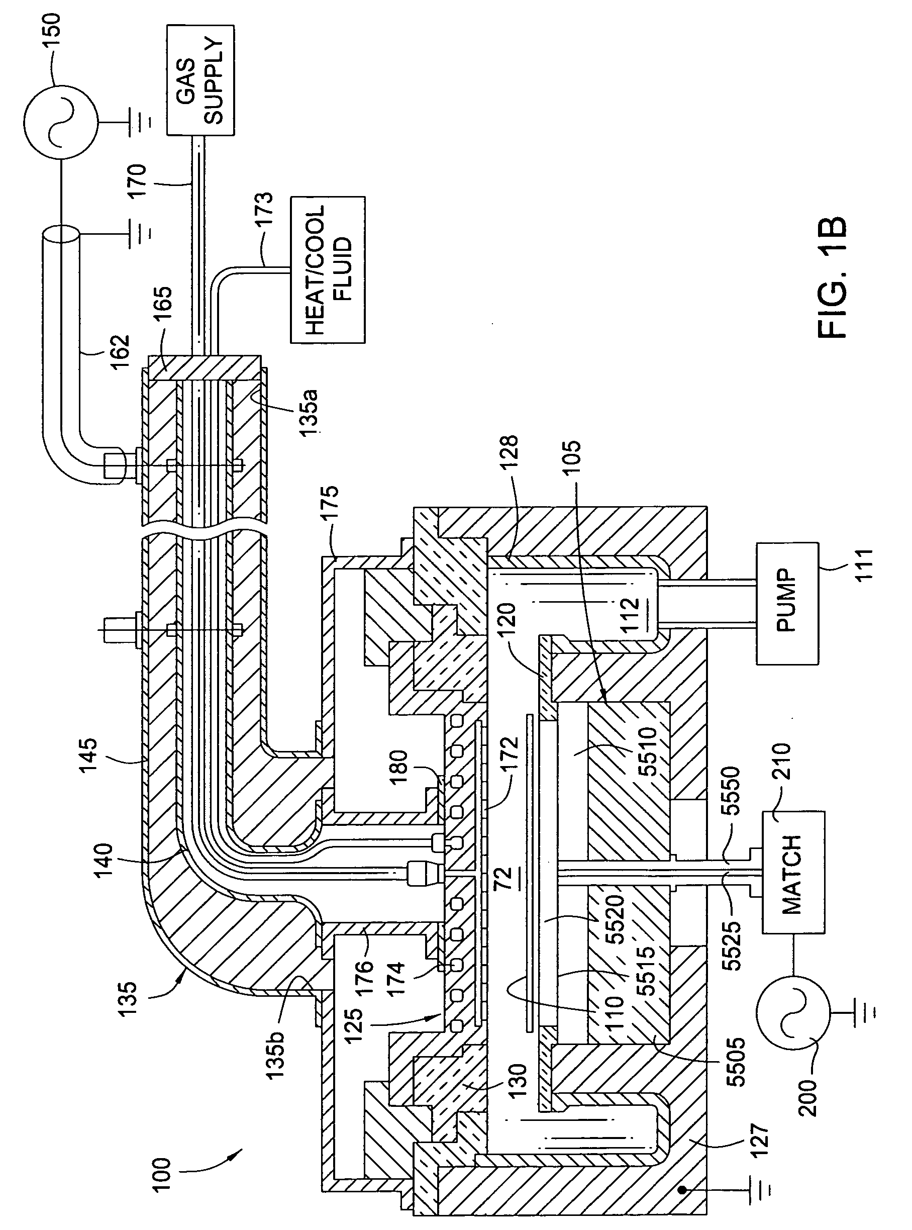
[0034]FIG. 1B illustrates an example of a plasma reactor, such as the Enabler® etch system manufactured by Applied Materials, Inc., of Santa Clara, Calif., that includes a reactor chamber 100, which may include liners to protect the walls, with a substrate support (or pedestal) 105 at the bottom of the chamber supporting a semiconductor wafer 110. The chamber 100 is bounded at the top by a disc shaped overhead aluminum elec...


PUM

PropertyMeasurementUnit
gap widthaaaaaaaaaa
chamber pressureaaaaaaaaaa
gap widthaaaaaaaaaa

Abstract

The embodiments of the present invention generally relate to a method and an apparatus to confine a plasma within a processing region in a plasma processing chamber. The apparatus may include an annular ring with a gap distance with the chamber wall at between about 0.8 inch to about 1.5 inch. In addition to the annular plasma confinement ring, the plasma can also be confined by reducing a voltage supplied to the top electrode by a voltage ratio during plasma processing and supplying the remaining voltage supplied to the top electrode at a negative phase at the substrate support and the substrate, if the substrate is present during processing. The voltage ratio can be adjusted by changing the impedances of the substrate support and the dielectric seal surrounding the top electrode. Lowering top electrode voltage by a voltage ratio and supplying the remaining voltage supplied to the top electrode at a negative phase at the substrate support reduce the amount of plasma got attracted to the grounded chamber walls and thus improves plasma confinement. This method of plasma confinement is called impedance confinement. Plasma confinement can be improved by using either the described annular ring, the impedance confinement scheme or a combination of both.

Description

FIELD OF THE INVENTION [0001] The embodiments of the present invention generally relate to method and apparatus to confine plasma and to enhance flow conductance in plasma processing reactors. BACKGROUND OF THE INVENTION [0002] Plasma processing of semiconductor wafers in the manufacture of microelectronic integrated circuits is used in dielectric etching, metal etching, chemical vapor deposition and other processes. In semiconductor substrate processing, the trend towards increasingly smaller feature sizes and line-widths has placed a premium on the ability to mask, etch, and deposit material on a semiconductor substrate, with greater precision. [0003] Typically, etching is accomplished by applying radio frequency (RF) power to a working gas supplied to a low pressure processing region over a substrate supported by a support member. The resulting electric field creates a reaction zone in the processing region that excites the working gas into a plasma. The support member is biased ...

Claims


Application Information

Patent Timeline
Patent Type & Authority Applications(United States)
IPC IPC(8): H01L21/302C23F1/00H01L21/461
CPCH01J37/32082H01J37/32623H01J37/32642Y10S156/915
Inventor BERA, KALLOLHOFFMAN, DANIELYE, YANKUTNEY, MICHAELBUCHBERGER, DOUGLAS A.
Owner APPLIED MATERIALS INC
Why Eureka
Try Eureka