Plasma processing apparatus

a processing apparatus and plasma technology, applied in the direction of coatings, chemical vapor deposition coatings, electric discharge tubes, etc., can solve the problems of difficult etching processing of these materials, pt and fe, and the likelihood of precipitation of high-volatile reaction products for precious metals, etc., to achieve stable and uniform plasma

Inactive Publication Date: 2006-08-10
HITACHI HIGH-TECH CORP
View PDF8 Cites 49 Cited by
  • Summary
  • Abstract
  • Description
  • Claims
  • Application Information

AI Technical Summary

Benefits of technology

[0025] The present invention has been devised in view of these problems. Accordingly, an object of the present invention is to provide a plasma processing apparatus which is capable of generating a stable and uniform plasma.

Problems solved by technology

These precious metals are considerably unlikely to form high-volatility reaction products.
Accordingly, it is extremely difficult to perform an etching processing for these materials.
However, the above-described materials such as Pt and Fe, which are materials to be newly introduced from now on, exhibit only a low reactivity with the halogen-containing gases.
It is not at all easy, however, to implement the plasma etching of these non-volatile materials at a mass-production level.
This deposition film changes the plasma state, or generates particles, thereby making the plasma etching processing difficult.
This decreases the plasma density, thereby giving rise to a decrease in the etching rate, or increasing the number of particles flying over onto the wafers.

Method used


Image

  • Plasma processing apparatus
  • Plasma processing apparatus
  • Plasma processing apparatus

Examples


Embodiment Construction

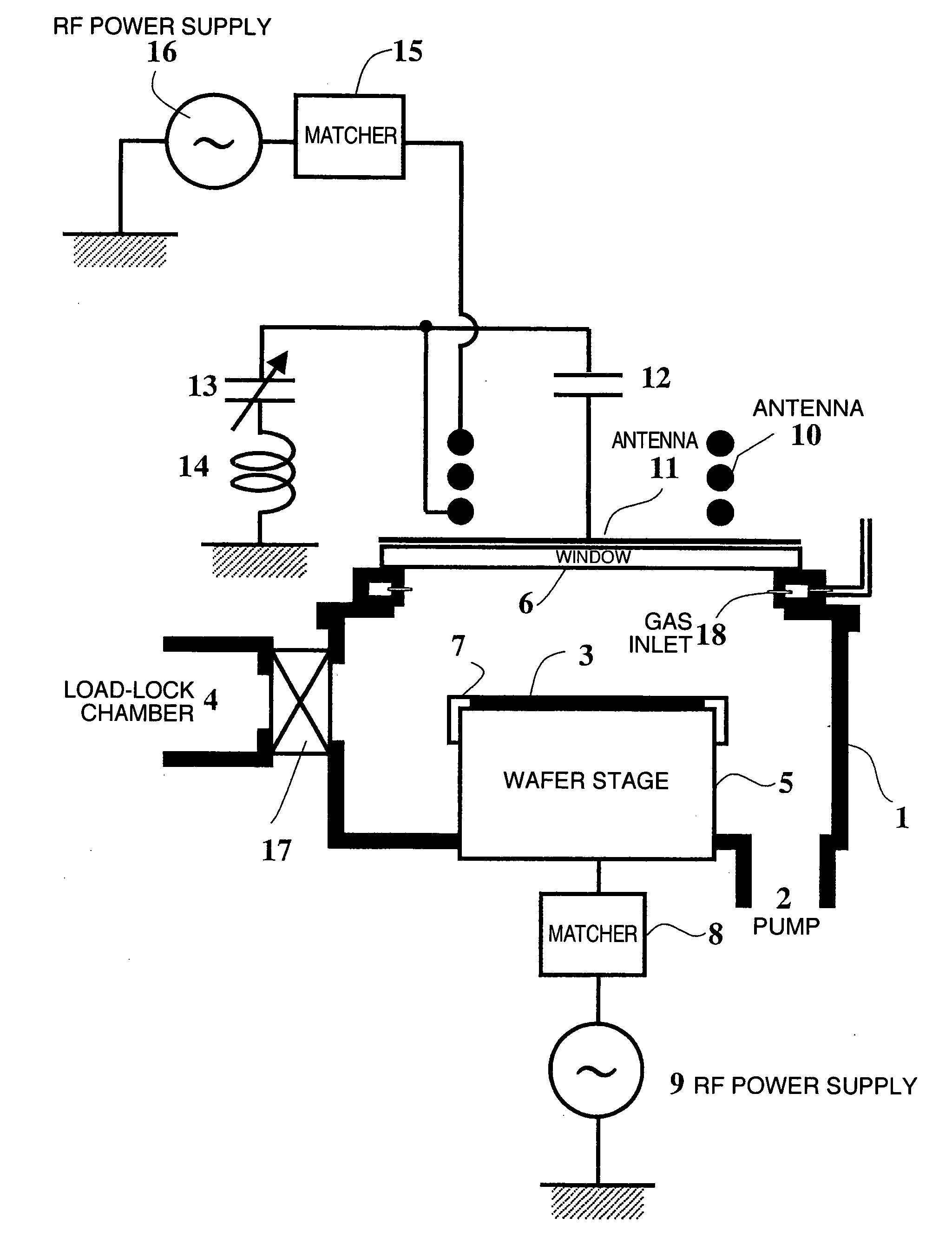
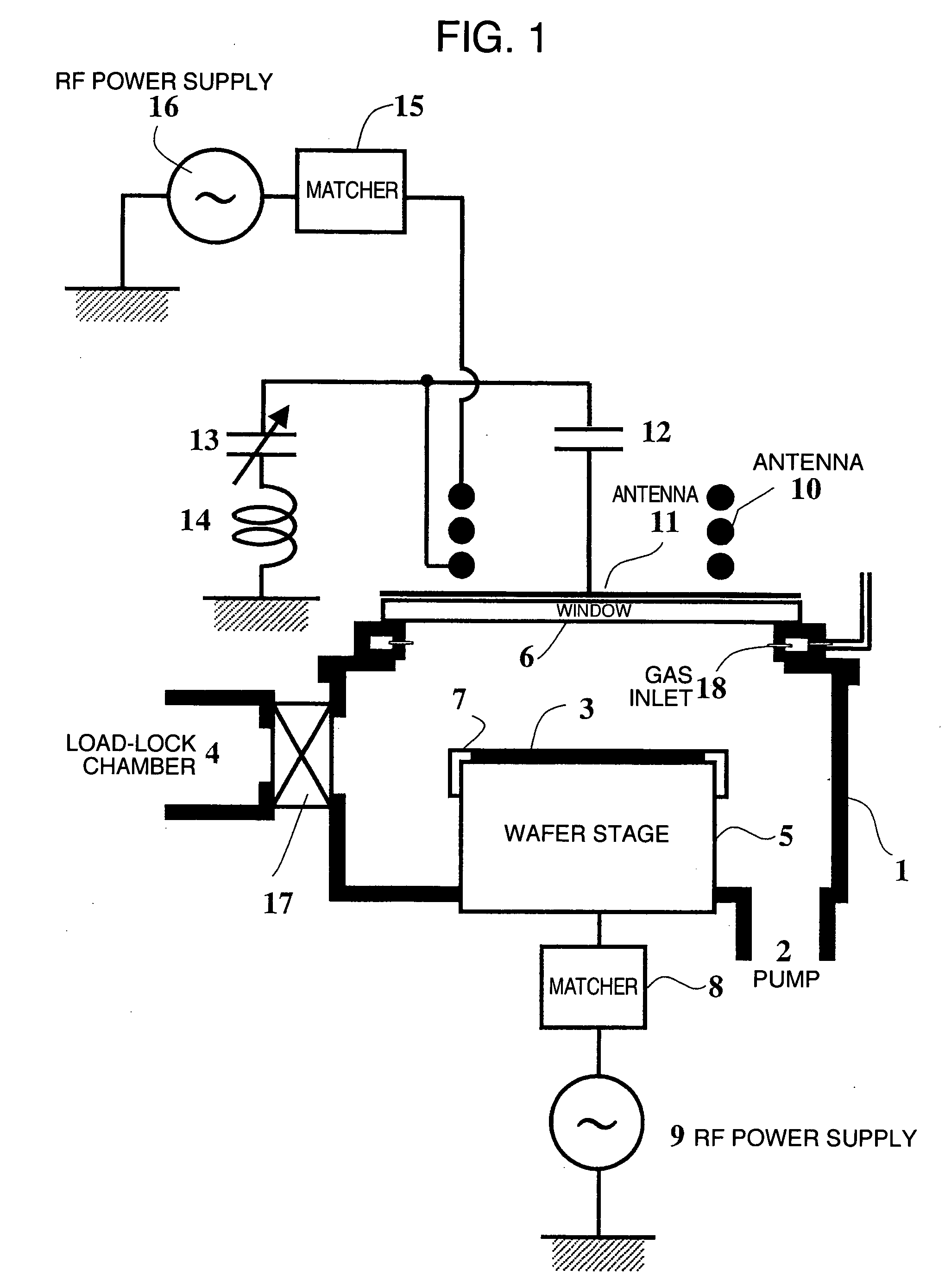
[0044] Hereinafter, referring to the accompanying drawings, the explanation will be given below concerning the best embodiments. FIG. 1 is a diagram for explaining a plasma processing apparatus according to the first embodiment of the present invention. In FIG. 1, a processing chamber 1 is, e.g., an aluminum-formed or stainless-formed vacuum container whose surface is subjected to an anodized processing. The processing chamber 1 is electrically grounded, and includes a pumping unit 2 and a transportation system 4 for transporting a semiconductor wafer 3, i.e., a specimen to be processed, into / from the processing chamber.

[0045] An electrode or stage 5 for mounting the semiconductor wafer 3 thereon is set inside the processing chamber 1. The wafer 3 is transported into the processing chamber by the transportation system 4 via a transporting gate valve 17. Moreover, the wafer 3 is conveyed onto the electrode 5, then being held by being chucked by a not-illustrated electrostatic chuck....


PUM

PropertyMeasurementUnit
temperatureaaaaaaaaaa
pressureaaaaaaaaaa
inclination angleaaaaaaaaaa

Abstract

A plasma processing apparatus capable of generating a stable and uniform-density plasma includes a processing chamber whose one surface is formed by a flat-plate-like insulating-material manufactured window, a sample mounting stage in which a sample mounting plane is formed on a surface opposed to the insulating-material manufactured window of the processing chamber, a gas-inlet for introducing a processing gas into the processing chamber, a flat-plate-structured capacitively coupled antenna formed on an outer surface of the insulating-material manufactured window with slits provided in a radial pattern, and an inductively coupled antenna formed outside the insulating-material manufactured window and performing an inductive coupling with a plasma via the window, the plasma being formed within the processing chamber. The inductively coupled antenna is configured by a coil which is wound a plurality of times with a direction defined longitudinally, the direction being perpendicular to the sample mounting plane.

Description

BACKGROUND OF THE INVENTION [0001] 1. Field of the Invention [0002] The present invention relates to a plasma processing apparatus. More particularly, it relates to a plasma processing apparatus which is capable of generating a stable and uniform plasma. [0003] 2. Description of the Related Art [0004] In recent years, in conventional LSI devices as well as in novel memory devices such as FeRAM (Ferroelectric Random Access Memory) and MRAM (Magnetoresistive Random Access Memory), much use has been made of materials such as precious metals, e.g., Pt and Ir, magnetic materials, and non-volatile materials. [0005] For example, a capacitor unit for storing bit information in FeRAM is configured such that a ferroelectric material such as PZT (Pb(Ti, Zr)O3) or SBT (SrBi2Ta2O9) is sandwiched between electrodes of the precious metals such as Ir, Ru, or Pt. These precious metals are considerably unlikely to form high-volatility reaction products. Accordingly, it is extremely difficult to perfo...

Claims


Application Information

Patent Timeline
Patent Type & Authority Applications(United States)
IPC IPC(8): C23F1/00C23C16/00
CPCH01J37/32091H01J37/321H01L21/67069
Inventor EDAMURA, MANABUYOSHIOKA, KENSHIMADA, TAKESHI
Owner HITACHI HIGH-TECH CORP
Why Eureka
Try Eureka