Substrate holding mechanism using electrostaic chuck and method of manufacturing the same

a technology of electrostaic chuck and substrate, which is applied in the direction of mechanical equipment, manufacturing tools, synthetic resin layered products, etc., can solve the problems of shortened service life of electrostatic fasteners and induced plasma so as to prevent corrosion of adhesive layers, prolong the service life of substrate processing apparatus, and ensure the protection of adhesive layers.

Inactive Publication Date: 2006-08-10
TOKYO ELECTRON LTD
View PDF7 Cites 26 Cited by
  • Summary
  • Abstract
  • Description
  • Claims
  • Application Information

AI Technical Summary

Benefits of technology

[0042] According to the present invention, for example, the adhesive layer may be protected from plasma and corrosion of the adhesive layer may be prevented. In this way, particle generation may be controlled and the service life of the substrate processing apparatus may be prolonged. It is particularly noted that by providing the convex portion, the adhesive layer may be protected, and by covering the periphery surface of the convex portion and the side surface of the first protection member with the second protection member, protection of the adhesive layer may be further ensured.

Problems solved by technology

However, in such a structure, a wafer is attracted and held by the ceramic film during substrate processing, and thereby, the ceramic material may come off and be attached to the wafer.
However, in a CVD apparatus or an etching apparatus according to the prior art including such a ceramic sheet that is bonded to the electrostatic attraction sheet using adhesive, when oxygen plasma or fluorine plasma is used, for example, corrosion of the adhesive layer may be induced by the plasma.
Also, the service life of the electrostatic fastener may be shortened due to such corrosion of the adhesive layer.

Method used


Image

  • Substrate holding mechanism using electrostaic chuck and method of manufacturing the same
  • Substrate holding mechanism using electrostaic chuck and method of manufacturing the same
  • Substrate holding mechanism using electrostaic chuck and method of manufacturing the same

Examples


first embodiment

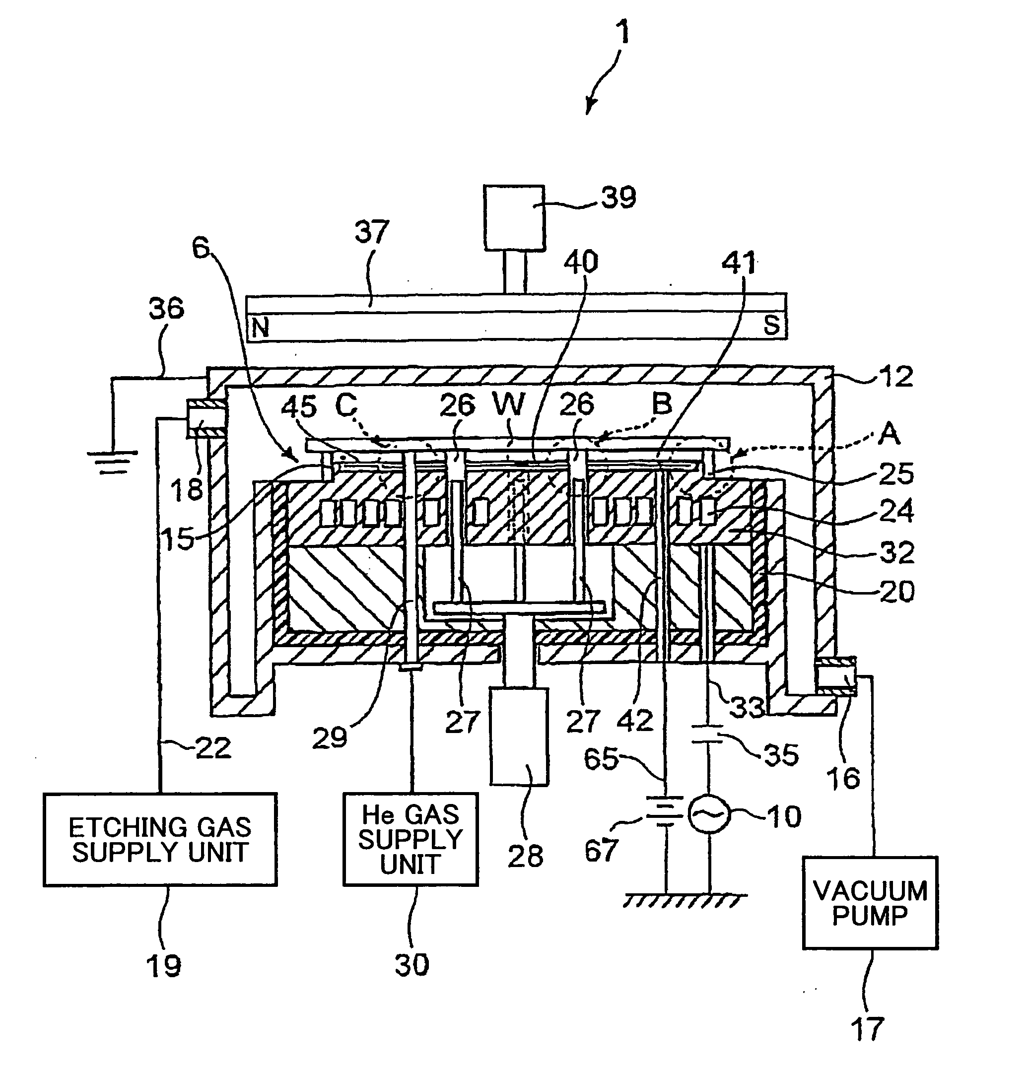
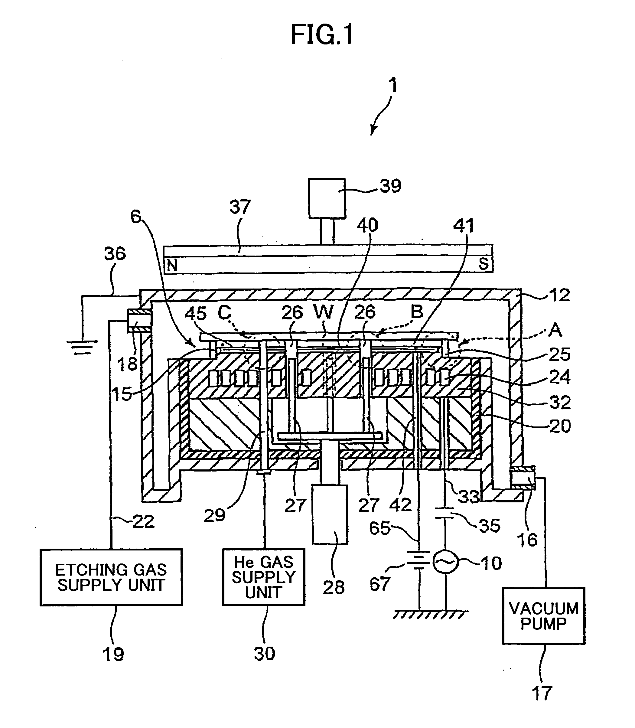
[0053]FIG. 1 is a cross-sectional view of a plasma etching apparatus including an electrostatic fastener according to an embodiment of the present invention. The plasma etching apparatus of FIG. 1 includes a vacuum chamber 12, a table 6 for supporting a wafer W within the vacuum chamber 12, a magnet unit 8, for example, that is used for forming a magnetic field in a direction orthogonal to an electric field within the vacuum chamber 12, and an RF power source 10 for generating plasma within the vacuum chamber 12.

[0054] It is noted that the vacuum chamber 12 also functions as a container wall.

[0055] An evacuation outlet 16 is arranged at the vacuum chamber 12, and a vacuum pump 17 is connected to the evacuation outlet 16. The pressure within the vacuum chamber 12 may be reduced to approximately 1˜100 Pa by the vacuum pump 17. Also, a gas inlet 18 for supplying etching gas is arranged at the vacuum chamber 12. The gas inlet 18 is connected to etching gas supply unit 19 via a supply ...

second embodiment

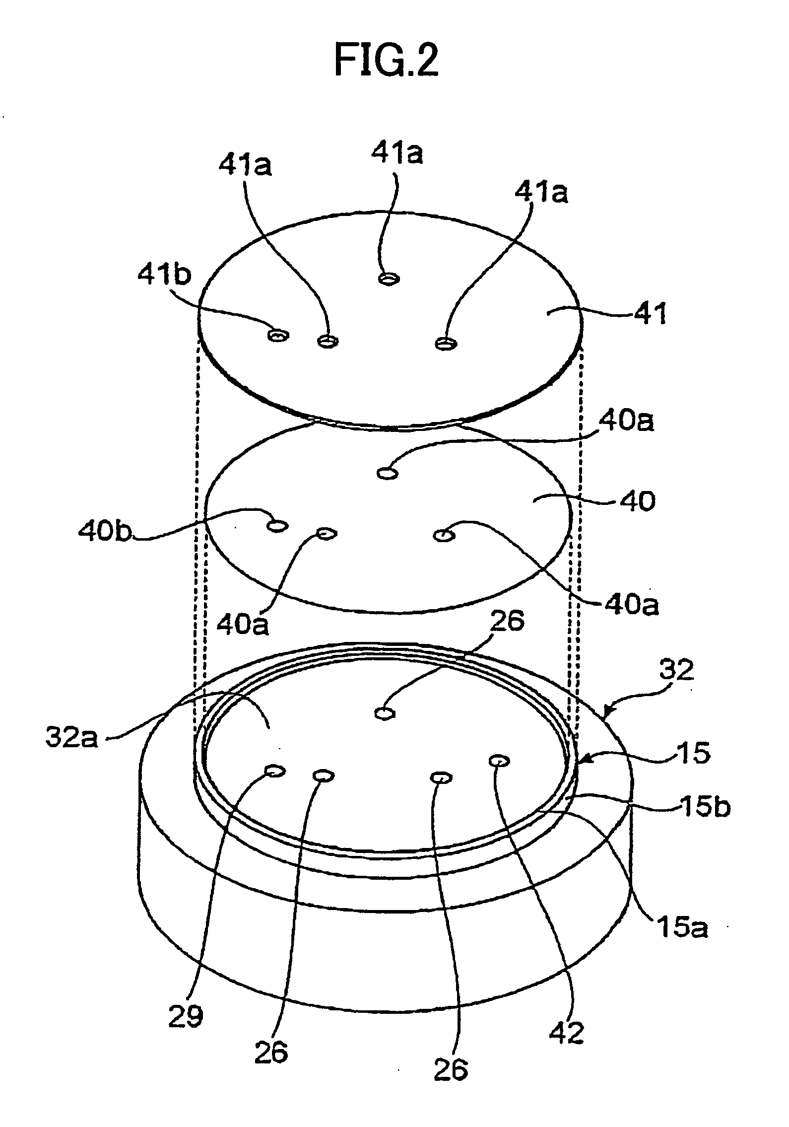
[0083]FIGS. 6, 7, 8, and 9 are enlarged cross-sectional views of portions of electrostatic fasteners according to other embodiments of the present invention. It is noted that the portions illustrated in these drawings correspond to the portion shown in FIG. 3 of the first embodiment.

[0084] Referring to FIG. 6, the electrostatic fastener according to the present embodiment includes a polyimide sheet 146 placed on a stage 132 via an adhesive layer 147, and a conductive sheet 145, placed on the polyimide sheet 146, covered by an adhesive layer 144. An adhesive layer 149 including such an electrostatic attraction sheet made up of the above layers is surrounded by another adhesive layer 71. In this way, a protective member 141 made of ceramic is attached to the stage 132 via the adhesive layer 149 and the adhesive layer 71. The adhesive layer 71 may include silicon, for example, and is preferably arranged to have relatively high resistance to oxygen plasma. In the case of using plasma d...


PUM

PropertyMeasurementUnit
widthaaaaaaaaaa
widthaaaaaaaaaa
widthaaaaaaaaaa

Abstract

A substrate holding apparatus includes a stage configured to support a substrate to be processed, the stage including a surface, and a continuous convex portion surrounding a predetermined region of the surface which convex portion includes a periphery surface and an upper surface that is positioned higher than the surface of the stage; an electrostatic attraction sheet configured to attract a substrate with electrostatic force, the electrostatic attraction sheet being arranged on the surface of the stage within the region surrounded by the convex portion; a first protection member configured to protect the electrostatic attraction sheet, the first protection member being arranged on the electrostatic attraction sheet and including a side surface and a portion that is arranged to face opposite the upper surface of the convex portion; an adhesive layer that is arranged at least between the electrostatic attraction sheet and the first protection member and is configured to bond the electrostatic attraction sheet and the first protection member; and a second protection member that covers at least the outer peripheral surface of the convex portion and the side surface of the first protection member to conceal at least the adhesive layer.

Description

TECHNICAL FIELD [0001] The present invention generally relates to a substrate processing apparatus that performs processes such as a CVD process and / or an etching process on a semiconductor substrate and a method of manufacturing the same. The present invention particularly relates to a substrate holding apparatus implementing an electrostatic fastener that is used for holding a substrate within such a substrate processing apparatus and a method of manufacturing the same. BACKGROUND ART [0002] Processes for manufacturing a semiconductor device include numerous steps. For example, a process for forming a circuit pattern on a semiconductor wafer (referred to as wafer hereinafter) may include a cleaning step for cleaning the wafer, a film formation step for forming metal films and / or insulating films, a photolithography step for forming a wiring pattern using a photo resist, an etching step for etching the wafer with the resist pattern formed thereon, and other various steps such as a ...

Claims


Application Information

Patent Timeline
Patent Type & Authority Applications(United States)
IPC IPC(8): B32B38/00H01L21/683
CPCY10T279/23H01L21/6833H01L21/68
Inventor NOZAWA, TOSHIHISA
Owner TOKYO ELECTRON LTD
Why Eureka
Try Eureka