Semiconductor device

a semiconductor device and semiconductor technology, applied in the direction of semiconductor devices, electrical devices, transistors, etc., can solve the problems of complex manufacturing process, no longer achieved performance improvement, and serious problems in capacitance reduction, etc., and achieve the effect of effective work function

Active Publication Date: 2006-08-17
KK TOSHIBA
View PDF3 Cites 21 Cited by
  • Summary
  • Abstract
  • Description
  • Claims
  • Application Information

AI Technical Summary

Benefits of technology

[0024]FIG. 4 is a graph showing an effective work function of a Ta simple substance and Ta compounds on HfSiON and SiO2;
[0025]FIG. 5 is a graph to exp

Problems solved by technology

However, in a complementary metal-insulator-semiconductor (CMIS) device in which gate length is 50 nm or less, performance improvement is no longer achieved when a conventional polysilicon gate electrode is used.
This capacitance reduction will be a serious problem in a CMIS technique generation in which the dielectric thickness is 2 nm or less.
However, when the gate electrodes of the nMISFET and the pMISFET are formed of different metals, it is necessary to individually produce the gate electrodes, which causes the problem that the manufacturing process is complicated and manufacturing costs increase.
Howeve

Method used


Image

  • Semiconductor device
  • Semiconductor device
  • Semiconductor device

Examples


first embodiment

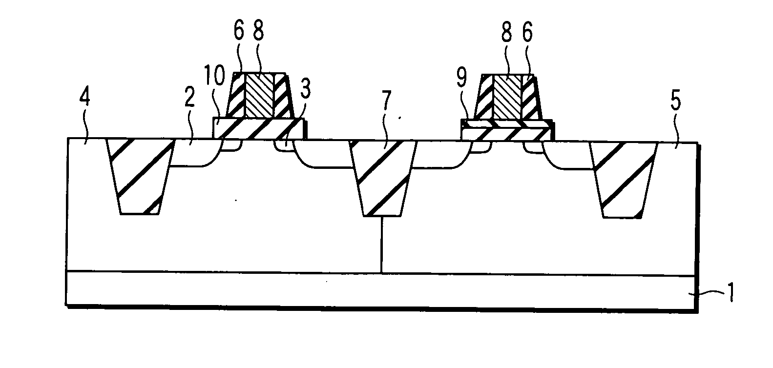
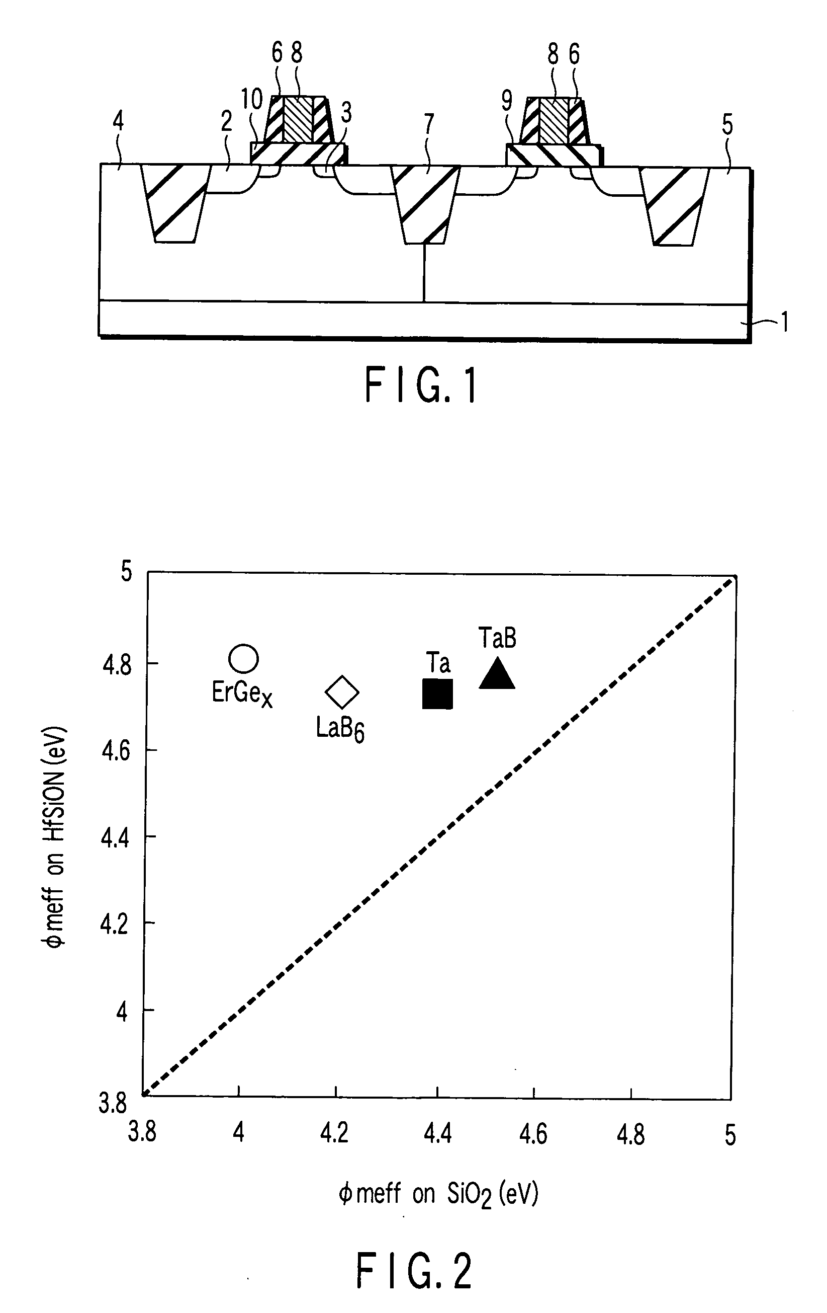
[0036]FIG. 1 is a sectional view of a semiconductor device according to a first embodiment of the present invention. In a surface region of an Si substrate as a semiconductor substrate, there are provided an n-type semiconductor region 4 and a p-type semiconductor region 5, and a pMISFET and an nMISFET are formed in the respective regions. The n-type, p-type semiconductor regions 4, 5 are formed as so-called wells.

[0037] On a surface of the n-type semiconductor region 4, a gate dielectric (insulating film) is formed which is made of an oxide 10 containing a metal atom having lower binding energy to combine with a metal atom of a gate electrode 8 than Al, Si and Ge. The metal atoms are, for example, Zr, Hf, Ti, Ta, Nb, V, Sc, Y, and a lanthanoide and actinide series.

[0038] On a surface of the p-type semiconductor region 5, a dielectric 9 different from the gate dielectric 10 is formed which includes any one of Al, Si and Ge having high binding energy to combine with the metal atoms...

second embodiment

[0069]FIG. 7 is a sectional view of a semiconductor device according to a second embodiment of the present invention. FIG. 8 is a schematic enlarged sectional view of an Si substrate, a gate dielectric and a gate electrode of a pMISFET in the semiconductor device of FIG. 7. A gate dielectric made of an oxide 10 is formed on an n-type Si substrate 4. A gate electrode 8 is formed on the gate dielectric 10. Although not shown, a refractory metal such as W or the like may further be formed on the gate electrode 8.

[0070]FIG. 9 is a schematic enlarged sectional view of an Si substrate, a gate dielectric and a gate electrode of an nMISFET in the semiconductor device of FIG. 7. A gate dielectric is formed on a p-type Si substrate. The second embodiment is different from the first embodiment in that the gate dielectric has a laminated structure, and a lower layer thereof includes the oxide 10 on which a dielectric 9 different from the lower layer is formed, as understood from FIG. 9. Other ...

third embodiment

[0080]FIG. 14 is a sectional view of a semiconductor device according to a third embodiment of the present invention. FIG. 15 is a schematic enlarged sectional view of an Si substrate, a gate dielectric and a gate electrode of a pMISFET in the semiconductor device of FIG. 14. A gate dielectric is formed on an n-type semiconductor region 4. The gate dielectric has a laminated structure, and a lower layer thereof is a dielectric 9. A dielectric 10 different from the lower layer is formed on the dielectric 9, and this is different from the first embodiment.

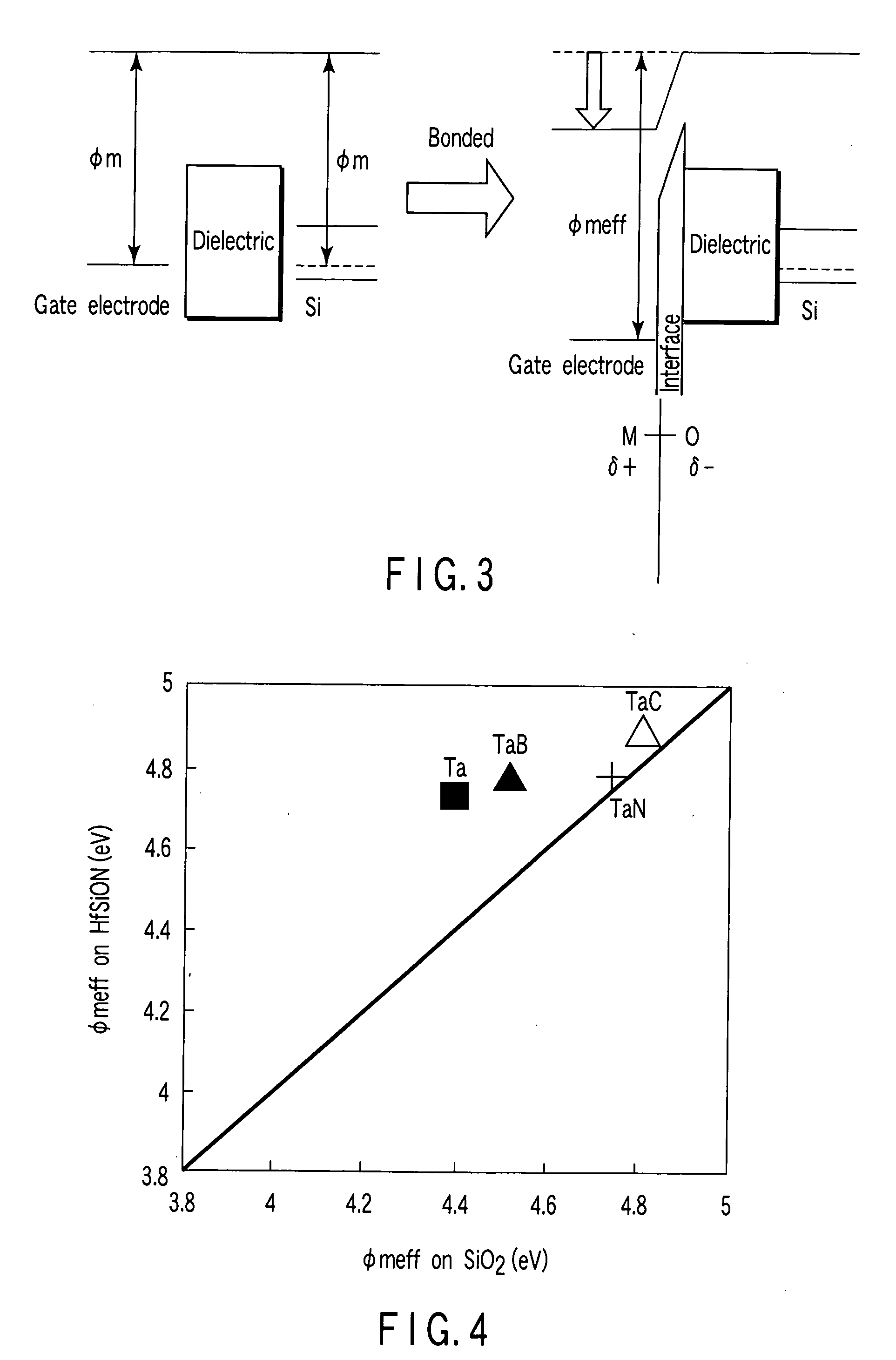
[0081] As described in the first embodiment, since a difference in the effective work function is caused by a dipole formed at an interface between the gate electrode and the gate dielectric, a thickness of the gate dielectric 10 is not limited, and the dielectric 10 may be any dielectric as long as it is one or more monolayers between the metal electrode and the oxide film 10. The gate dielectric 10 needs to be as thin as possible ...


PUM


Abstract

A semiconductor device includes a semiconductor substrate, an nMISFET formed on the substrate, the nMISFET including a first dielectric formed on the substrate and a first metal gate electrode formed on the first dielectric and formed of one metal element selected from Ti, Zr, Hf, Ta, Sc, Y, a lanthanoide and actinide series and of one selected from boride, silicide and germanide compounds of the one metal element, and a pMISFET formed on the substrate, the pMISFET including a second dielectric formed on the substrate and a second metal gate electrode formed on the second dielectric and made of the same material as that of the first metal gate electrode, at least a portion of the second dielectric facing the second metal gate electrode being made of an insulating material different from that of at least a portion of the first dielectric facing the first metal gate electrode.

Description

CROSS-REFERENCE TO RELATED APPLICATIONS [0001] This application is based upon and claims the benefit of priority from prior Japanese Patent Application No. 2005-036575, filed Feb. 14, 2005, the entire contents of which are incorporated herein by reference. BACKGROUND OF THE INVENTION [0002] 1. Field of the Invention [0003] The present invention relates to a semiconductor device, and more particularly to a structure of a CMIS semiconductor device using a metal gate electrode. [0004] 2. Description of the Related Art [0005] As miniaturization of MISFETs progresses to improve integration and performance of semiconductor devices, it is necessary to reduce a thickness of a gate dielectric (insulating film). However, in a complementary metal-insulator-semiconductor (CMIS) device in which gate length is 50 nm or less, performance improvement is no longer achieved when a conventional polysilicon gate electrode is used. This is because the equivalent SiO2 thickness of the gate dielectric is ...

Claims


Application Information

Patent Timeline
IPC IPC(8): H01L29/76H01L21/28H01L21/283H01L21/8238H01L27/092H01L29/423H01L29/49
CPCH01L21/823462H01L21/823857H01L29/51H01L29/511H01L29/517
Inventor ICHIHARA, REIKATSUCHIYA, YOSHINORIKOYAMA, MASATONISHIYAMA, AKIRA
Owner KK TOSHIBA
Why Eureka
Try Eureka