Signal line driving circuit and image display device

a driving circuit and signal line technology, applied in the field of signal line driving circuits, can solve the problems of increasing power consumption in the signal line driving circuit, and achieve the effects of reducing the parasitic capacitance of wiring and the number of elements, and extending the operation margin

Inactive Publication Date: 2006-08-17
SHARP KK
View PDF11 Cites 14 Cited by
  • Summary
  • Abstract
  • Description
  • Claims
  • Application Information

AI Technical Summary

Benefits of technology

[0012] An object of the present invention is to provide (i) a signal line driving circuit which can reduce parasitic capacitance of wiring and the number of elements, and miniatualize an amplitude of an input signal; and (ii) a low-power-consumption-type image display device which affords a broader operation margin and which can reduce a burden of an external interface, by having such a signal line driving circuit.
[0016] In the foregoing structure, the switching element controls input of the width specifying pulse, and since it is the shift pulse that holds such control, for example, when the switching element becomes OFF while the shift pulse is non-active, a signal line transmitting the width specifying pulse will be disconnected from the signal line driving circuit, thereby reducing capacitive load due to the signal line, and, consequently, power consumption. As a result, it is possible to realize lower power consumption and faster operation of the signal line driving circuit with ease.
[0023] In the foregoing structure, since the scanning signal line driving circuit includes the signal line driving circuit, the power consumption of the scanning signal line driving circuit can be reduced. In the image display device in particular, because the proportion of the power consumption of the driving circuit is large with respect to the entire power consumption, it is effective to attain lower power consumption of the scanning line driving circuit. Additionally, in the signal line driving circuit, since capacitive load of the signal line for transmitting the width specifying pulse is reduced as described above, it is possible to broaden the operation margin. Further, miniatualization of the signal line driving circuit by reducing the number of elements is effective to reduce the size of an edge portion where the driving circuit is provided in the image display device, and consequently, an image display device with reasonable cost, low running cost and a high-performance can be provided.

Problems solved by technology

This is one of the factors that causes the increase in power consumption in the signal line driving circuits.

Method used


Image

  • Signal line driving circuit and image display device
  • Signal line driving circuit and image display device
  • Signal line driving circuit and image display device

Examples


first embodiment

[0039] The following will describe the first embodiment of the present invention with reference to FIGS. 1 and 2.

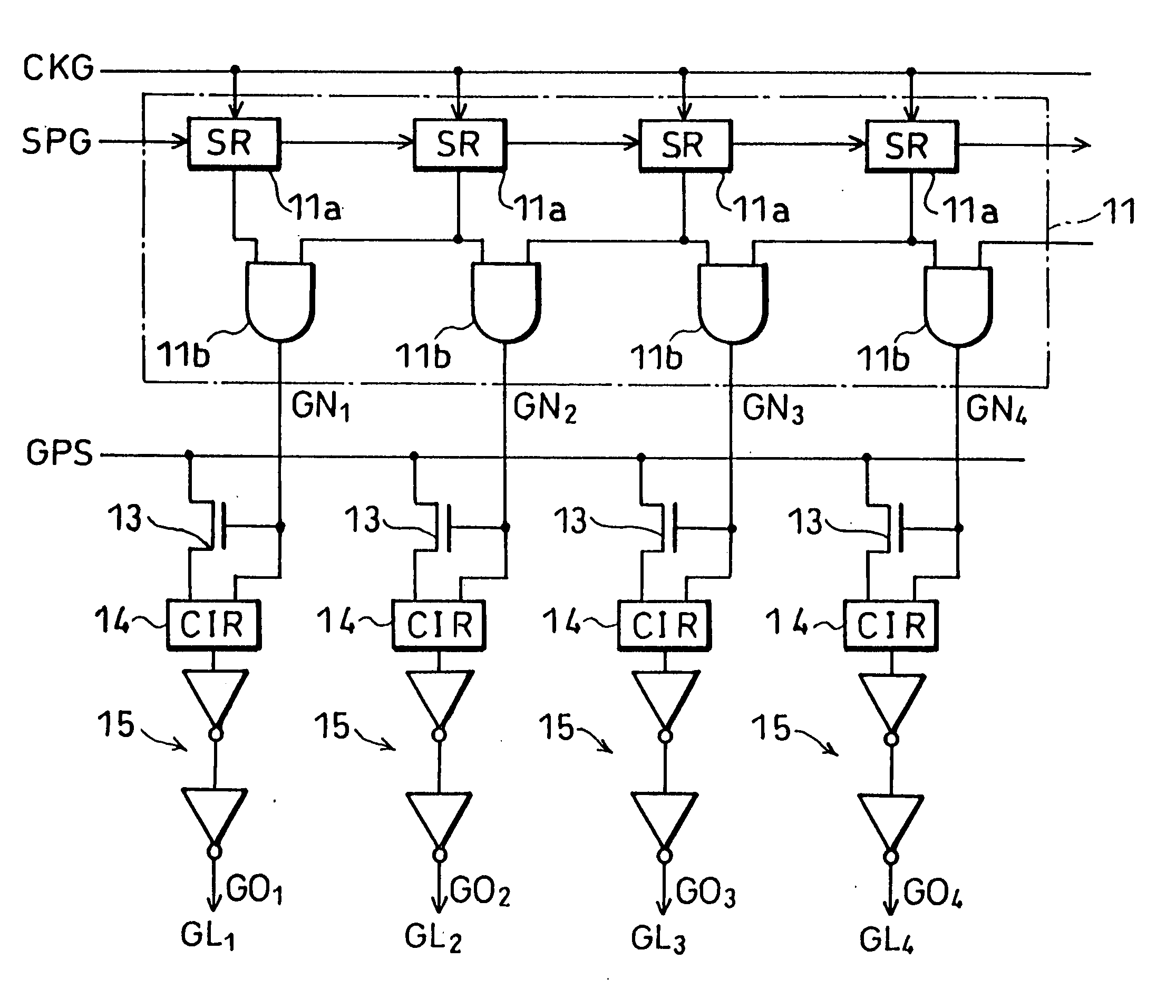
[0040] As shown in FIG. 1, the signal line driving circuit according to the present embodiment includes a shift register 11, transistors 13, logical operation circuits (CIR as illustrated) 14 and buffer circuits 15.

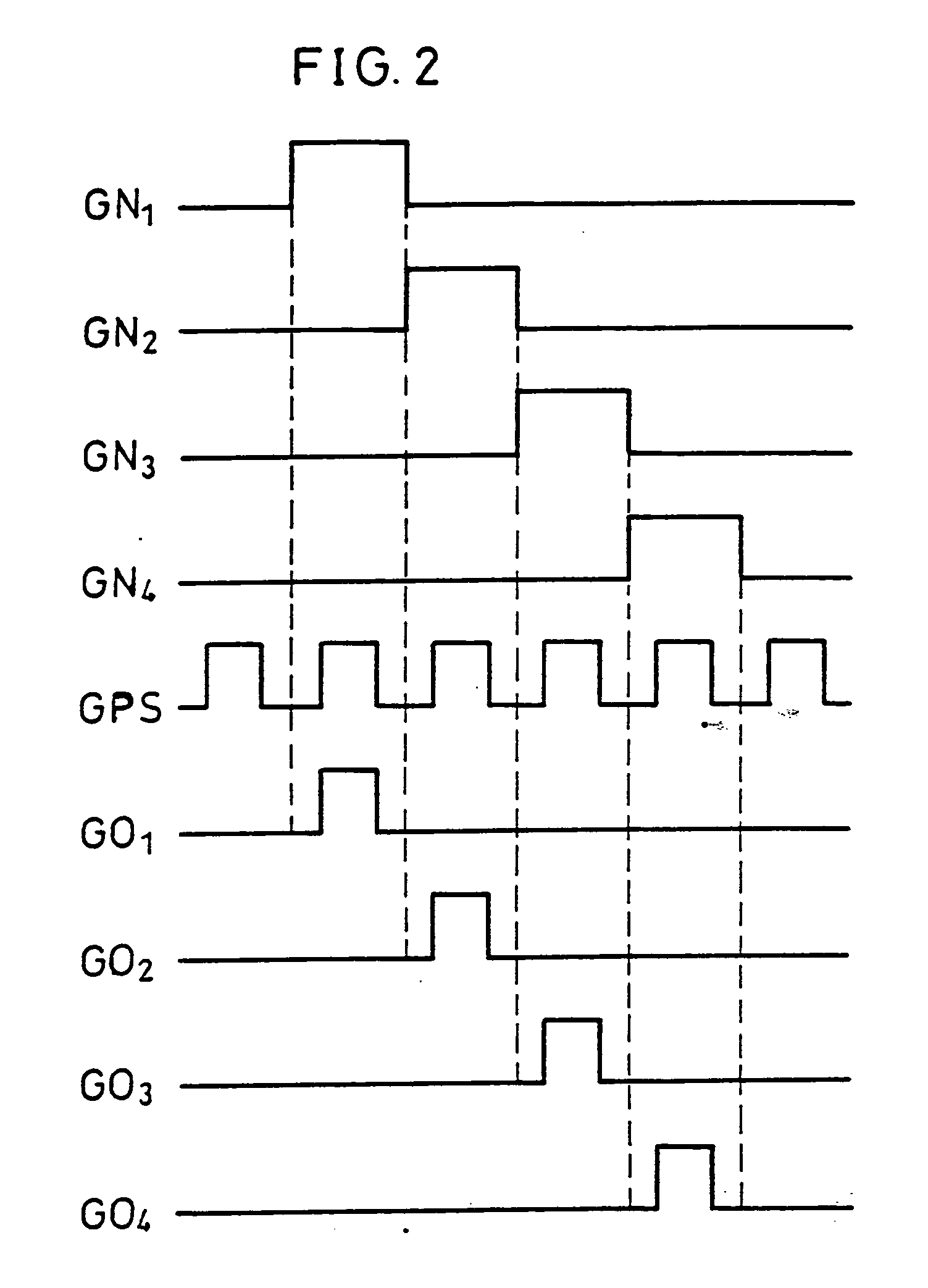
[0041] The shift register 11 has a plurality of shift circuits 11a and AND gates 11b, of which the shift circuits 11a are serially connected to one another. The shift circuit 11a shifts an externally inputted start pulse SPG subsequently to the shift circuit 11a on the next stage based on a clock signal CKG. The AND gate 11b outputs a logical product of the pulses outputted from two adjacent shift circuits 11a, as the shift pulse GNn (n=1, 2, 3 . . . ).

[0042] Note that, the shift register 11 may exclude the AND gates 11b. In this structure; a pulse outputted from each shift circuit 11a becomes the shift pulse GNn.

[0043] In FIG. 1, the transistor 13 is an n-...

second embodiment

[0050] The following will explain the second embodiment of the present invention with reference to FIG. 3. Note that, for convenience of explanation, in the following embodiments including the present embodiment, the elements having the same or equivalent functions to those already discussed in the first embodiment above will be given the same reference numerals, and explanation thereof will be omitted here.

[0051] The signal line driving circuit in accordance with the present embodiment includes, as shown in FIG. 3, the shift register 11, the transistors 13 and the buffer circuits 15, as with the first embodiment. However, the logical operation circuits 14 are omitted. Specifically, the transistor 13 here is directly connected to the buffer circuit 15 without interference of the logical operation circuit 14.

[0052] With the structure as above, the width specifying pulse GPS is outputted via the transistor 13 while the transistor 13 is ON, i.e. while the shift pulse GNn is active (s...
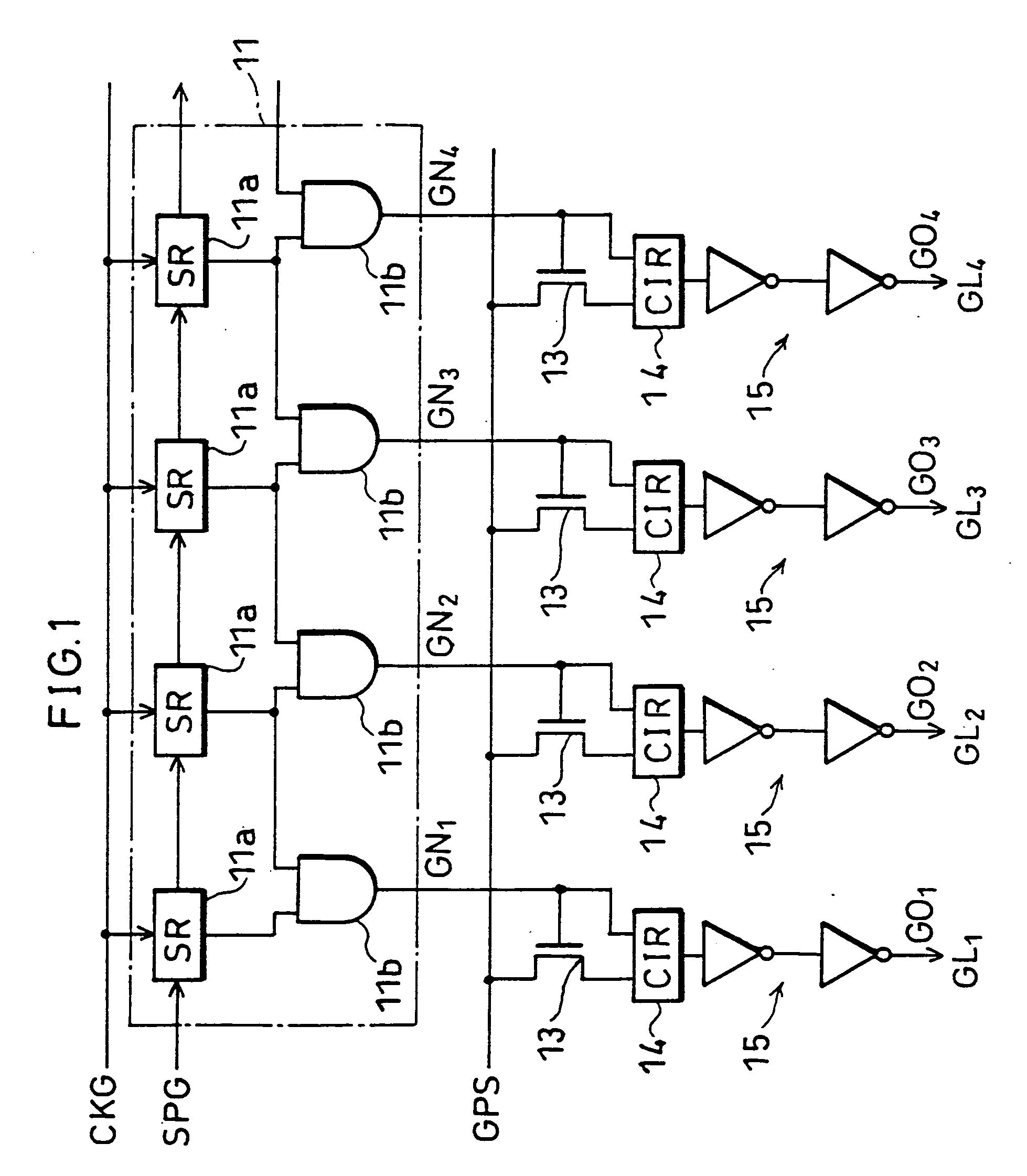
third embodiment

[0056] The following will explain the third embodiment of the present invention with reference to FIG. 4.

[0057] As shown in FIG. 4, the signal line driving circuit in accordance with the present embodiment includes the shift register 11, the buffer circuits 15, as with the signal line driving circuit of the first embodiment (see FIG. 1), except for inverters 21 and transfer gates 22, which are provided instead of the transistors 13 and the logical operation circuits 14.

[0058] The transfer gate 22 is a switching element of a CMOS structure, composed of an n-channel transistor 22a and a p-channel transistor 22b which are connected to each other in parallel. To the gate of the n-channel transistor 22a is inputted the shift pulse GNn, and to the gate of the p-channel transistor 22b is inputted the shift pulse GNn which has been inverted by the inverter 21. Accordingly, the transfer gate 22 becomes ON when the shift pulse GNn is active, and the width specifying pulse GPS is outputted. ...


PUM

PropertyMeasurementUnit
widthaaaaaaaaaa
areaaaaaaaaaaa
capacitanceaaaaaaaaaa

Abstract

A signal line driving circuit includes a shift register having a plurality of shift circuits, each of which shifts a start pulse successively to the next stage, synchronizing with the timing of a clock signal. In this signal line driving circuit, shift pulses are outputted from an AND gate based on output pulses of two adjacent shift circuits. Meanwhile, a width specifying pulse for specifying a pulse width of the shift pulse is inputted via a transistor whose ON / OFF operation is controlled by the shift pulse. A logical operation circuit operates an AND of the shift pulse and the width specifying pulse and outputs the result of operation to a signal line. When the shift pulse is non-active, the transistor becomes OFF, which causes the signal line transmitting the width specifying pulse to be disconnected from the signal line driving circuit, thereby reducing a capacitive load of wiring. As a result, reduction of a parasitic capacitance of the wiring, reduction in the number of elements, reduction in the size of an amplitude of an input signal, etc. in the signal line driving circuit are attained.

Description

FIELD OF THE INVENTION [0001] The present invention relates to a signal line driving circuit that drives signal lines so as to supply signals to their destinations, and particularly to a simplification of a driving circuit used in image display devices, and in particular liquid crystal display devices. BACKGROUND OF THE INVENTION [0002] A signal line driving circuit of the present invention is applicable to a variety of systems. The following will describe the case where the signal line driving circuit is applied to an image display device, and in particular to an active-matrix type liquid crystal display device. However, the signal line driving circuit according to the present invention is not just limited to this, and evidently, it is equally effective in the other image display devices or systems, wherein the present invention is applicable. [0003] As a kind of conventional image display devices, liquid crystal display devices of an active-matrix driving system are known. As show...

Claims


Application Information

Patent Timeline
Patent Type & Authority Applications(United States)
IPC IPC(8): G09G3/36G02F1/133G09G3/20H04N5/66G11C19/00H03K17/693
CPCG09G3/3677G09G2310/0289
Inventor KUBOTA, YASUSHIWASHIO, HAJIMEMAEDA, KAZUHIROCAIRNS, GRAHAM ANDREWBROWNLOW, MICHAEL JAMES
Owner SHARP KK
Why Eureka
Try Eureka