Plating method

a metal film and plating technology, applied in the direction of dielectric characteristics, coatings, liquid/solution decomposition chemical coatings, etc., can solve the problems of limiting the applicability of this technique, difficult deposition of metal films, and limiting the applicability of metal film deposition

Inactive Publication Date: 2006-08-17
ROHM & HAAS ELECTRONICS MATERIALS LLC
View PDF14 Cites 32 Cited by
  • Summary
  • Abstract
  • Description
  • Claims
  • Application Information

AI Technical Summary

Problems solved by technology

Difficulties arise in the deposition of the metal films when the substrate has a complex surface profile, such as a curved surface or a three-dimensional surface.
Other difficulties arise when the substrate surface has recesses or cavities.
Such deposition processes typically require a reduced pressure environment which limits their

Method used


Image

  • Plating method
  • Plating method
  • Plating method

Examples


example 1

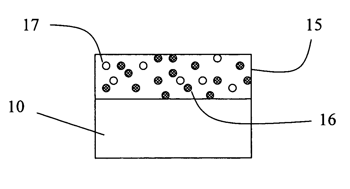
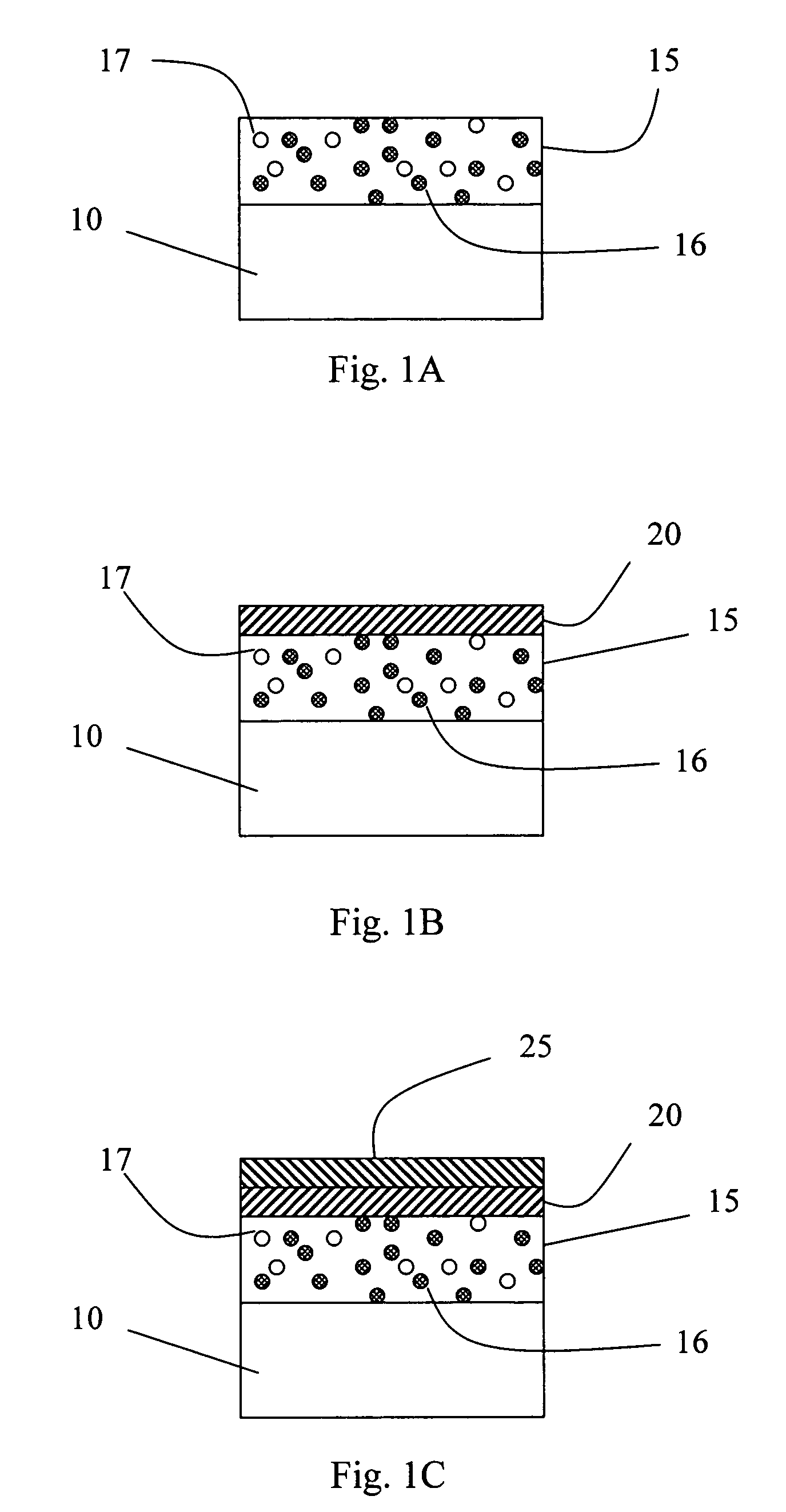
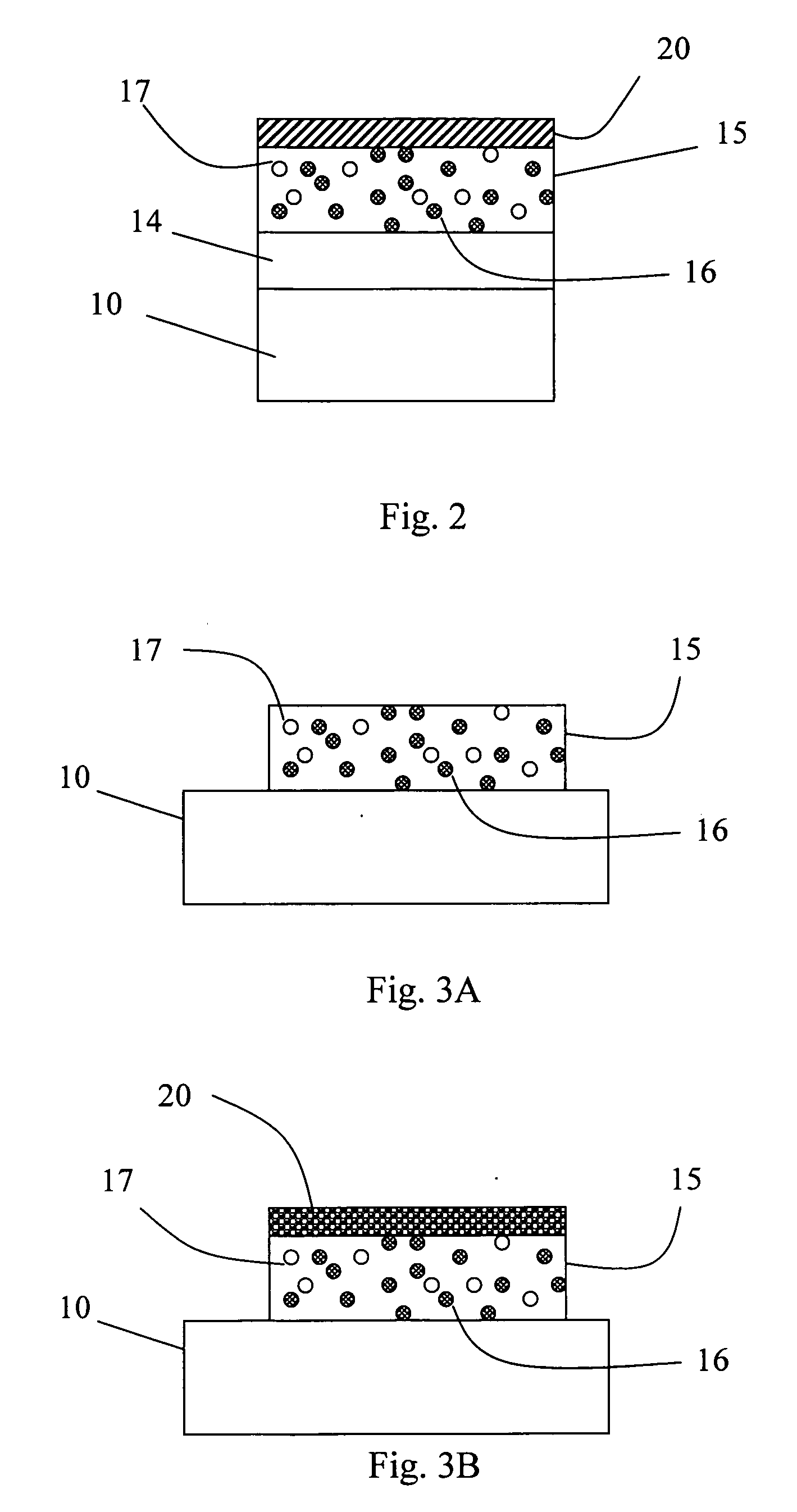
[0067] A 10 cm×10 cm glass substrate was cleaned as follows: contacting with isopropanol at 20° C. for 5 min., rinsing with cold water at 20° C. for 5 min., contacting with a 1% w / w solution of tetramethyl ammonium hydroxide in water at 50° for 5 min., rinsing with cold water at 20° C. for 4 min., and drying with compressed air and in an oven (120° C. for 10 min.).

[0068] An underlayer composition was prepared containing 6 wt % of phenyl-methyl silsesquioxane oligomer having the general formula (C6H5SiO1.5)(CH3SiO1.5), 0.5 wt % of a siloxane containing surfactant, the balance being propylene glycol monomethyl ether acetate.

[0069] An adhesion promoting composition was prepared containing 1 wt % of phenyl-methyl silsesquioxane oligomer having the general formula (C6H5SiO1.5)(CH3SiO1.5), 0.5 wt % of a siloxane containing surfactant, 20 g / L of palladium acetate as a plating catalyst, and 20 wt % of a porogen including as polymerized units methoxy-capped polypropylene oxide methacrylate...

example 2

[0072] The nickel plated sample from Example 1 was contacted with a commercially available electrolytic copper plating bath (EP 1100, available from Rohm and Haas Electronic Materials) using recommended plating conditions. After 2 minutes, the sample was removed from the plating bath and dried in air. A layer of copper (approximately 125 nm thick) was deposited on the electroless nickel layer.

example 3

[0073] The process of Example 1 was repeated. The electroless nickel plated sample was then contacted with a commercially available electroless copper plating bath (CIRCUPOSIT 880, available from Rohm and Haas Electronic Materials) using recommended plating conditions. Copper was deposited on the nickel layer at a rate of 8-12 nm / min. After removal from the plating bath, the sample was dried at 110° C. for 10 minutes and then annealed at 120° C. for 60 minutes. The sample contained a layer of electroless copper deposited on the layer of electroless nickel.


PUM

PropertyMeasurementUnit
Fractionaaaaaaaaaa
Fractionaaaaaaaaaa
Fractionaaaaaaaaaa

Abstract

Methods of improving the adhesion of metal layers to a substrate, such as an optical substrate, are provided. Such methods employ a layer of an adhesion promoting composition including a plating catalyst on the substrate before metal deposition. Also provided are devices made by such processes.

Description

BACKGROUND OF THE INVENTION [0001] The present invention relates generally to the field of metal plating. In particular, the present invention relates to the field of forming metal films on non-conductive substrates. [0002] In the manufacture of electronic devices such as liquid crystal display (“LCD”) devices, thin metal films are sometimes deposited as electrodes or circuitry on a substrate. Difficulties arise in the deposition of the metal films when the substrate has a complex surface profile, such as a curved surface or a three-dimensional surface. Other difficulties arise when the substrate surface has recesses or cavities. The surface profiles are typically reflected in the surface of the metal film which could result in recesses or cavities in the metal film. [0003] These metal films are often deposited on non-conductive surfaces, such as optical substrates. Such metal films are deposited by a variety of techniques such as vacuum evaporation, sputtering and chemical vapor de...

Claims


Application Information

Patent Timeline
IPC IPC(8): B05D5/06B05D1/36
CPCC23C18/1651C23C18/1851C23C18/1893C23C18/2086C23C18/1865H05K3/387H05K2201/0116H05K2201/0212H05K2201/0236C25D5/54C23C18/18C23C18/16
Inventor MONTANO, JOSEPH R.REESE, JASON A.LITTLE, LUKE W.
Owner ROHM & HAAS ELECTRONICS MATERIALS LLC
Why Eureka
Try Eureka