

Sputter-deposited rare earth element-doped silicon oxide film with silicon nanocrystals for electroluminescence applications
- Summary
- Abstract
- Description
- Claims
- Application Information
AI Technical Summary
Benefits of technology
Problems solved by technology
Method used
Image

Examples
Embodiment Construction
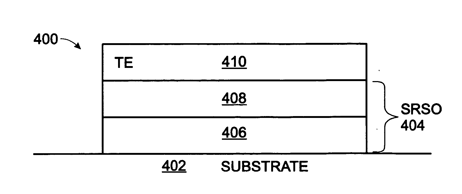
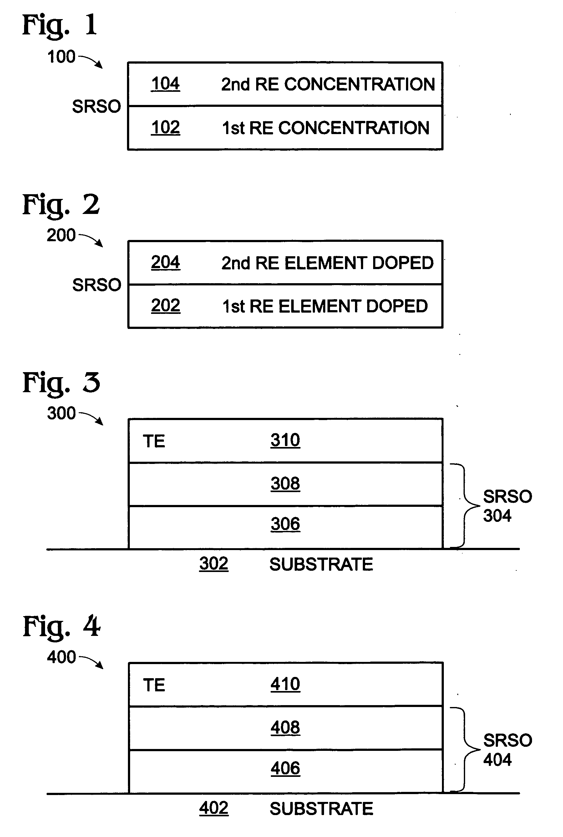
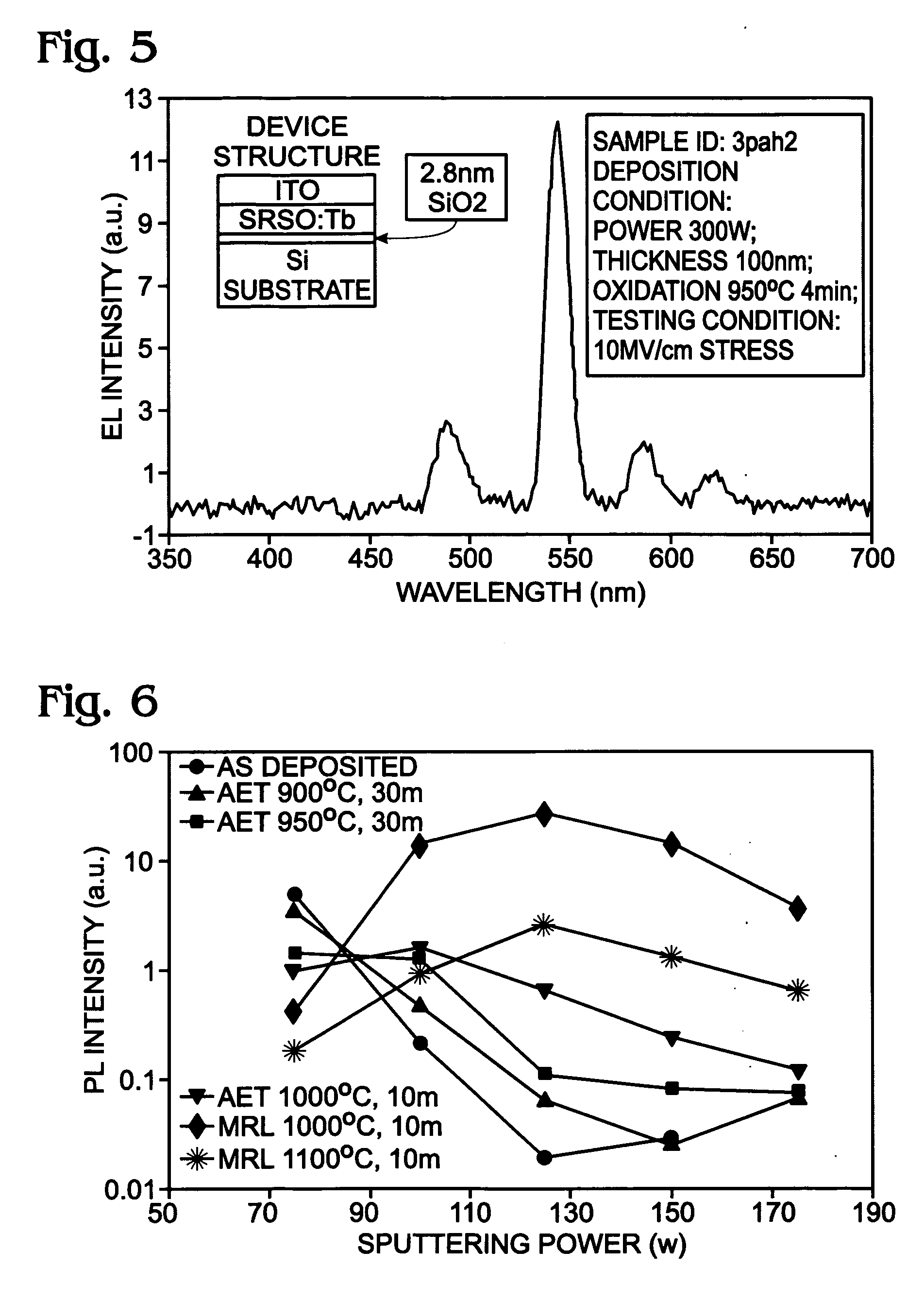
[0022]FIG. 1 is a partial cross-sectional view of a silicon-rich silicon oxide (SRSO) film. The SRSO film 100 comprises a first thickness 102 doped with a first concentration of a rare earth (RE) element. A second thickness 104, overlies the first thickness 102, and is doped with a second concentration of the RE element. In one aspect, the first concentration of RE dopant is greater than the second concentration. In another aspect, the second concentration of RE dopant is greater than the first. The film of FIG. 1 is intended to depict a simple exemplary RE doping profile that can be obtained using a two-target sputtering process to deposit the RE-doped SRSO film 100. Other, more complicated, profiles may be created using the same basic methodology.
[0023] As in all the SRSO films described below, SRSO film 100 is primarily silicon dioxide, with extra Si. After annealing, the Si atoms agglomerate together to form Si nano particles imbedded in a silicon oxide matrix. The silicon rich...
PUM
 Abstract
Description
Claims
Application Information