

Thin film semiconductor device, method of manufacturing the same, and display
- Summary
- Abstract
- Description
- Claims
- Application Information
AI Technical Summary
Benefits of technology
Problems solved by technology
Method used
Image

Examples
Embodiment Construction
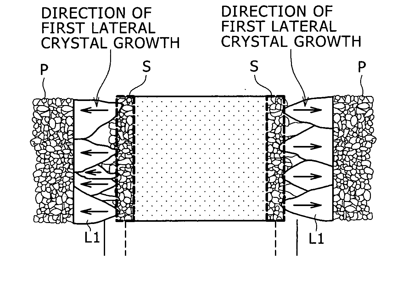
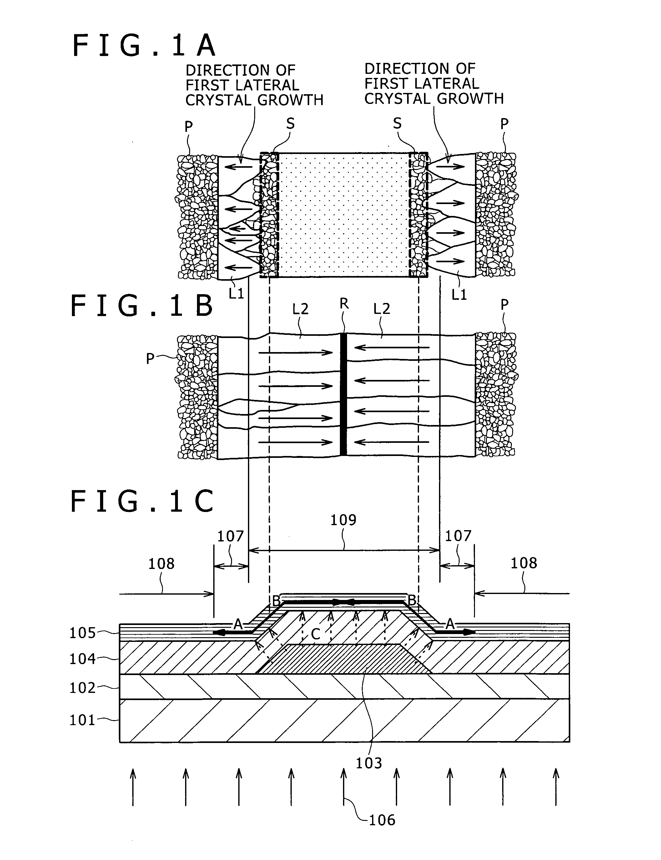
[0028] Now, embodiments of the present invention will be described in detail below, referring to the drawings. FIGS. 1A to 1C are schematic diagrams showing major points of the method of manufacturing a thin film semiconductor device according to the present invention, in which FIG. 1C are schematic sectional diagram of the semiconductor device, and FIGS. 1A and 1B are plan diagrams showing a phase change of a semiconductor thin film appearing in the manufacturing process. Basically, the method of manufacturing a thin film semiconductor device according to the present invention includes a light absorbing layer forming step, a patterning step, an insulation film forming step, a semiconductor thin film forming step, and a laser annealing step. As shown in FIG. 1C, in the light absorbing layer forming step, first, a light absorbing layer 103 is formed on the face side of a transparent substrate 101 formed of a glass or the like. In this embodiment, a thermal buffer layer 102 is prelimi...
PUM
 Abstract
Description
Claims
Application Information