Method for improving accuracy of MOSFET models used in circuit simulation integrated circuits

a technology of integrated circuits and mosfets, applied in error detection/correction, program control, instruments, etc., can solve the problems of inability to represent the actual shape of the mosfet in one rectangle, loss of accuracy, and inability to accurately predict etc., to achieve the effect of convenient implementation and accurate prediction of the performance of the mos

Inactive Publication Date: 2006-08-24
AXELRAD VALERY +1
View PDF3 Cites 8 Cited by
  • Summary
  • Abstract
  • Description
  • Claims
  • Application Information

AI Technical Summary

Benefits of technology

[0014] The present invention overcomes the limitations of prior art by providing a method for modeling submicron MOSFETs, capable of accurately predicting performance of a MOSFET with complex geometry closely approximating the actual geometry of a device manufactured as part of an integrated circuit. At the same time it provides a sub-circuit representation of a MOSFET that is equivalent to a regular MOSFET circuit model when ideal rectangular device geometry is assumed. Advantageously, the models created using the disclosed method are compatible with standard circuit simulators. The method may be readily implemented as part of a SPICE or other circuit simulation in a design flow. Such simulation may be employed to analyze circuits comprising analog and digital designs, and to study both nominal and statistical circuit performance as well as interaction between circuit and physical design and manufacturing process. This method readily lends itself to be implemented as a part of Design For Manufacturability (DFM) flow.
[0018] 3) generating a new set of parameter values for MOSFET models in such a way that new sub-circuit representation of the original MOSFET is electrically equivalent to the original MOSFET model when ideal rectangular geometry is assumed, while accurately capturing effects of non-ideal shape of real as-manufactured MOSFETs.
[0019] The present invention provides flexibility in the choice of simulation tools and simulation flow such that any SPICE-compatible or other circuit simulator can be used for subsequent simulations using MOSFET sub-circuit models created by present invention. Additionally there is no limitation as to which device-models can be used by the circuit simulator since the disclosed method makes no explicit assumption about the specific type of the MOSFET models used for each sub-circuit element. Further, the original structure and hierarchy of the SPICE model may also be maintained, allowing drop-in integration of the present invention in a design flow.

Problems solved by technology

However, as MOSFET process technology moves deeper into the submicron region, the accuracy of circuit simulation using common circuit simulation tools such as SPICE in combination with standard compact device models such as BSIM3 / 4, greatly diminishes.
The loss of accuracy occurs because the commonly used SPICE transistor models do not accurately capture 3-D effects, which become increasingly important in modern manufacturing processes.
In general, the actual shape of the MOSFET is however substantially more complex and cannot be represented by one rectangle.
2) Compact models do not accurately account for edge effects related to the manufacturing process, post-manufacturing mechanical stress or other narrow width effects.
Excessive complexity of the resulting sub-circuit would significantly increase simulation times and may create numerical problems with existing circuit simulators making it impossible to use them in practical simulations.

Method used


Image

  • Method for improving accuracy of MOSFET models used in circuit simulation integrated circuits
  • Method for improving accuracy of MOSFET models used in circuit simulation integrated circuits
  • Method for improving accuracy of MOSFET models used in circuit simulation integrated circuits

Examples


Embodiment Construction

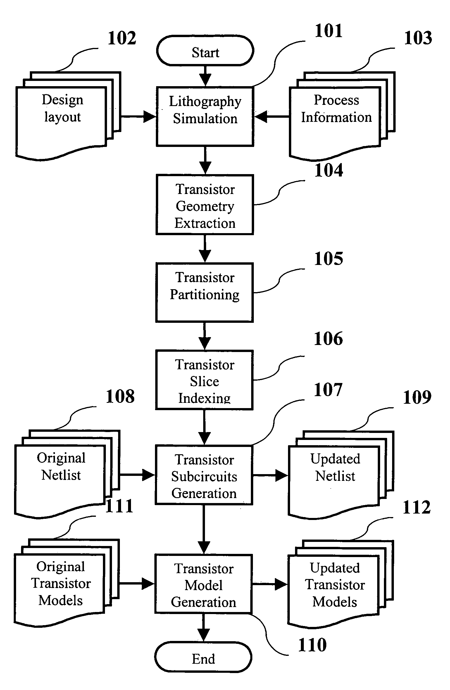
[0026]FIG. 1 depicts flow chart of a method of the invention. The flow begins at step 101 with lithography simulation. Lithography simulation uses input data in the form of the design layout 102 and lithographic process information 103 to predict final shapes of layout elements, which define transistor geometry.

[0027] Design layout 102 can be presented in any standard format such as GDS-II.

[0028] Process information 103 is a complete set of parameters characterizing the photolithography process which may include light source parameters such as wavelength and partial coherence, stepper parameters such as numerical aperture, aberrations and misalignment, as well as photoresist development and etch process parameters. Exact number of parameters characterizing lithographic process varies depending on the specifics of the lithographic process itself and models used to simulate the process.

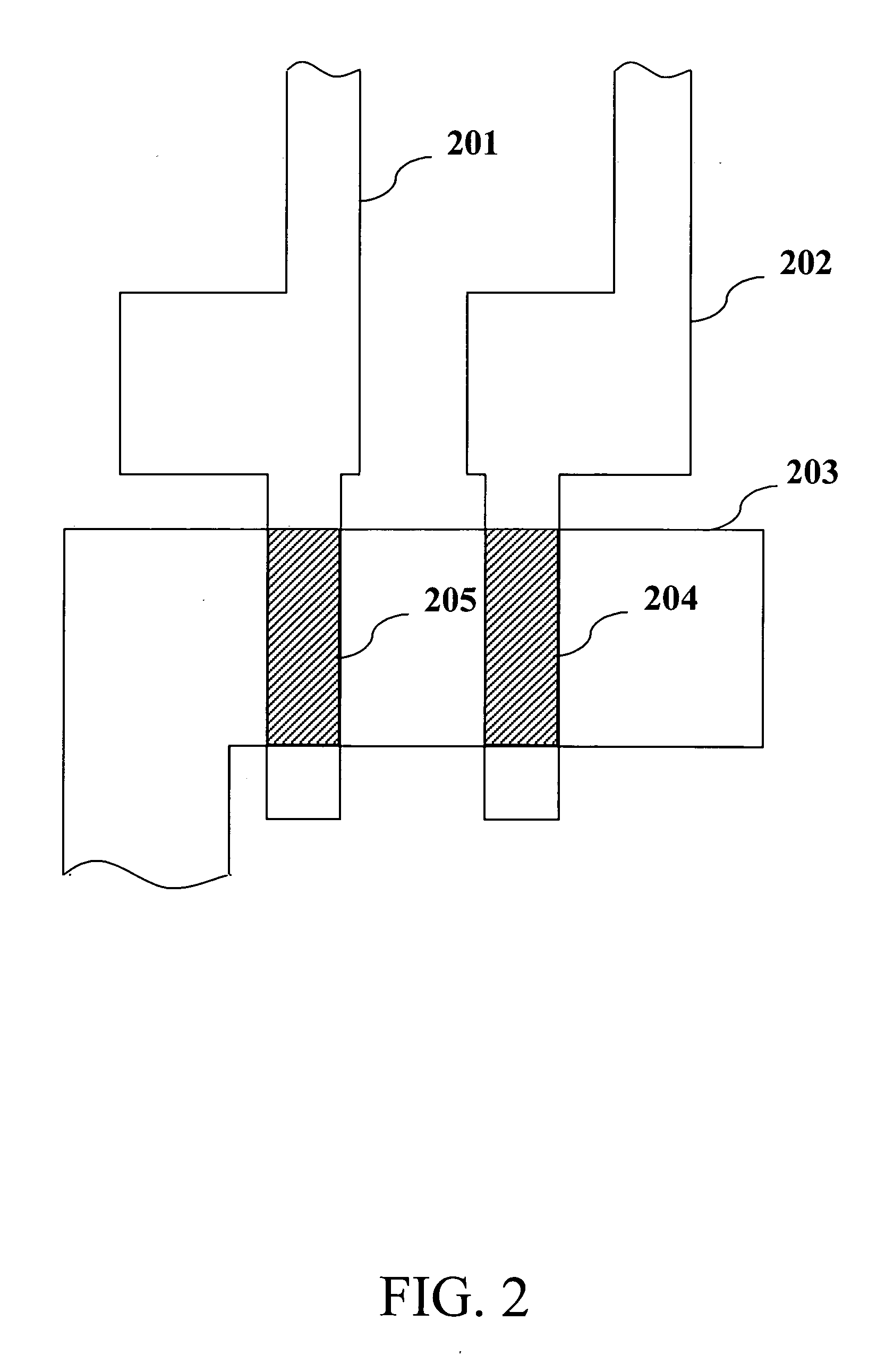
[0029]FIG. 2 presents a part of a typical integrated circuit layout in which polysilicon layer po...


PUM


Abstract

Disclosed is a method of modeling submicron MOSFETs for the purpose of circuit simulation. This invention is capable of accurately predicting performance of a MOSFET with complex geometry closely approximating the actual geometry of a device manufactured as part of an integrated circuit. Actual device geometry is predicted using physical simulation to account for process-related pattern distortion. The method constructs a sub-circuit representation of a MOSFET that is equivalent to a regular MOSFET compact model when ideal device geometry is assumed, while providing substantially better accuracy when process-related geometry distortion is considered. Models created using the disclosed method are compatible with existing circuit simulators. The method may be readily implemented using SPICE or other circuit simulators in a design flow.

Description

CROSS-REFERENCE TO RELATED APPLICATIONS [0001] This patent application is claiming the benefit of a prior filed provisional application Ser. No. 60 / 651,695, filed on Feb. 9, 2005, entitled “System and method for improving accuracy of MOSFET models used in circuit simulation of integrated circuits”.BACKGROUND OF THE INVENTION [0002] 1. Field of the Invention [0003] The present invention relates generally to integrated circuit development, modeling and simulation and more specifically to improving accuracy of MOSFET models used in circuit simulation of integrated circuits. [0004] 2. Description of Related Art [0005] An indispensable tool in the design of integrated circuits is the method of circuit simulation. The most familiar and commonly used circuit simulation tool is Berkeley SPICE and its commercial derivatives. [0006] To run SPICE or other circuit simulation, the circuit designer provides a) a description of the circuit known as the netlist, b) chooses models for the various ci...

Claims


Application Information

Patent Timeline
Patent Type & Authority Applications(United States)
IPC IPC(8): G06F17/50
CPCG06F17/5036G06F30/367
Inventor AXELRAD, VALERYSHIBKOV, ANDREI
Owner AXELRAD VALERY
Why Eureka
Try Eureka