Optical head, optical information storage apparatus, and their fabrication method

a technology of optical information storage and fabrication method, which is applied in the manufacture of optical heads, instruments, data recording, etc., can solve the problems of reducing the size of the optical head, difficult to handle such components for assembly or adjustment purposes, and the objective lens is difficult to adjust, so as to achieve the effect of low cost, accurate manufacturing in large quantities, and increased magnification of the optical system

Inactive Publication Date: 2006-08-31
HITACHI LTD
View PDF2 Cites 14 Cited by
  • Summary
  • Abstract
  • Description
  • Claims
  • Application Information

AI Technical Summary

Benefits of technology

[0028] Because the optical head of the invention is manufactured with the lenses, mirrors, prisms, light sources, and photodetectors already disposed on the wafers, and adjustments are made with reference to alignment marks or the like, ultra-small optical heads can be manufactured accurately in large quantities at low cost without requiring the handling of small components for adjustment purposes.
[0029] By causing the light beam to be incident on the detector after being reflected by the bottom and top surfaces of the prism / mirror substrate once or more, the magnification of the optical system can be increased while the thickness of the prism / mirror substrate is reduced.

Problems solved by technology

However, as the lens becomes smaller in size, other optical components must also be reduced in size, which would make it very difficult to handle such components for assembly or adjustment purposes.
In Patent Document 1, although the semiconductor laser, photodetector, and prism are combined, the objective lens is not, which is not quite advantageous in terms of minimization of the optical system.
Further, the prism must be individually affixed, resulting in a difficulty in handling and an increased time for adjustment, thereby making it difficult to achieve reduction in manufacturing cost.
In Patent Document 2, the objective lens is not integrated, as in Patent Document 1, and therefore this prior art is not suitable for the minimization of the optical system as a whole.
Further, with regard to the prism, complex laminated prisms must be individually adjusted and affixed to a semiconductor laser / photodetector module, resulting in an increased adjustment time and manufacturing cost.
In Patent Document 3, although the objective lens is integrated, the number of components is large and adjustment is difficult, such that reduction of manufacturing cost is difficult to achieve.
Particularly, it is difficult to secure sufficient positioning accuracy for the diffraction grating because it is disposed in an upright manner in the optical system.

Method used


Image

  • Optical head, optical information storage apparatus, and their fabrication method
  • Optical head, optical information storage apparatus, and their fabrication method
  • Optical head, optical information storage apparatus, and their fabrication method

Examples


embodiment 1

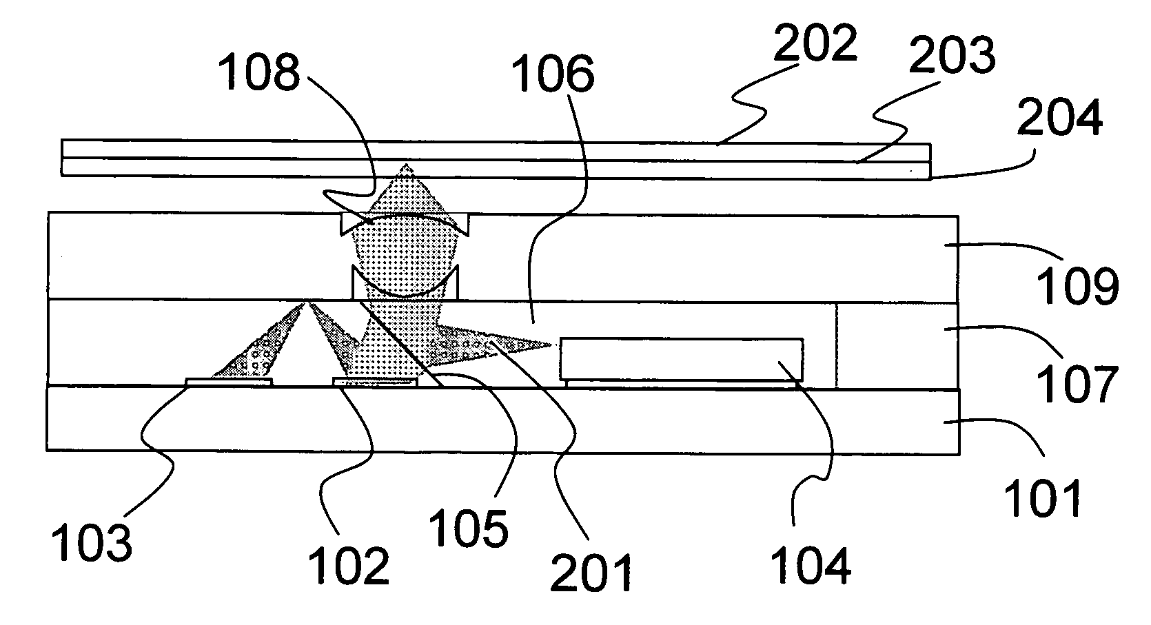
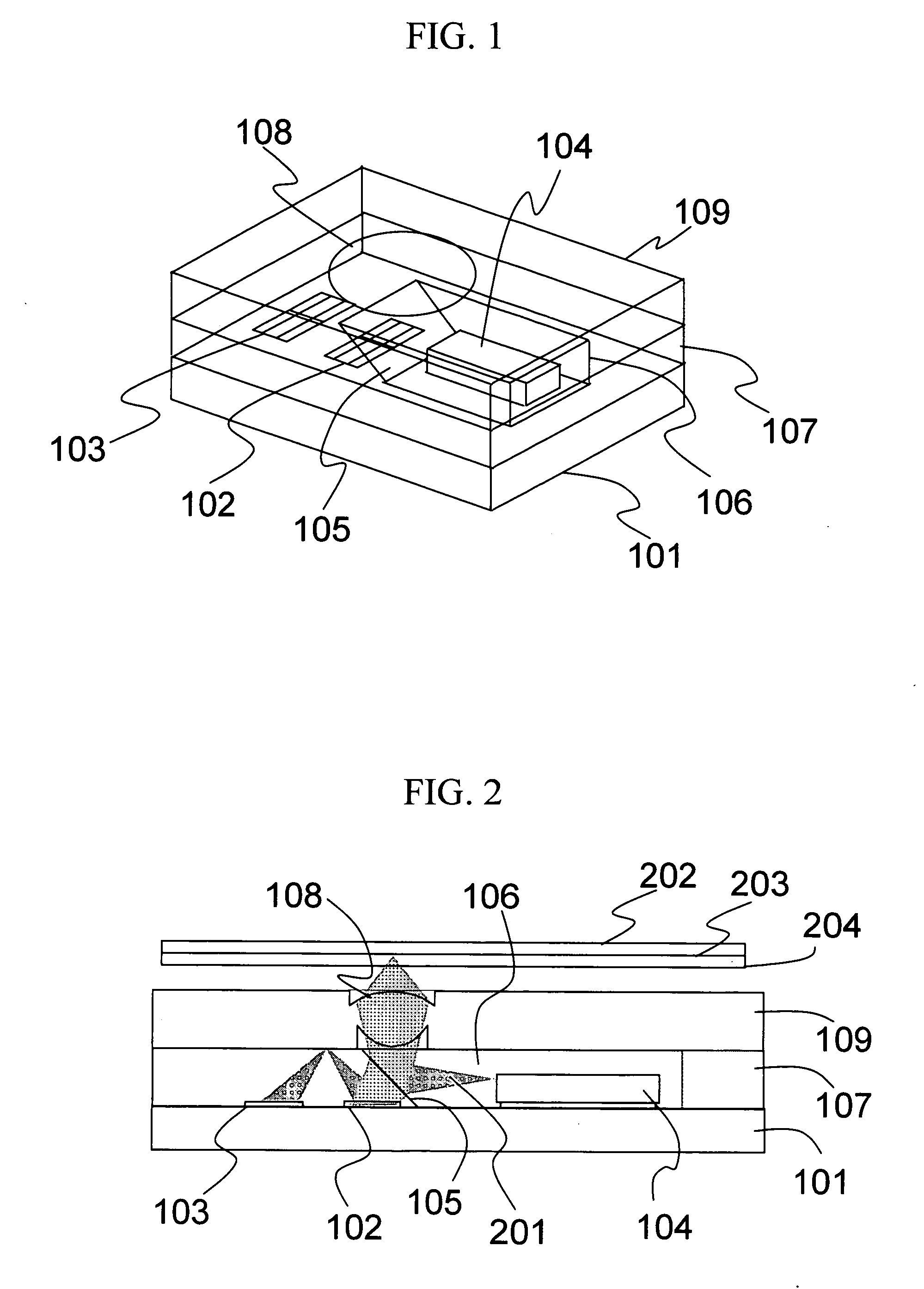
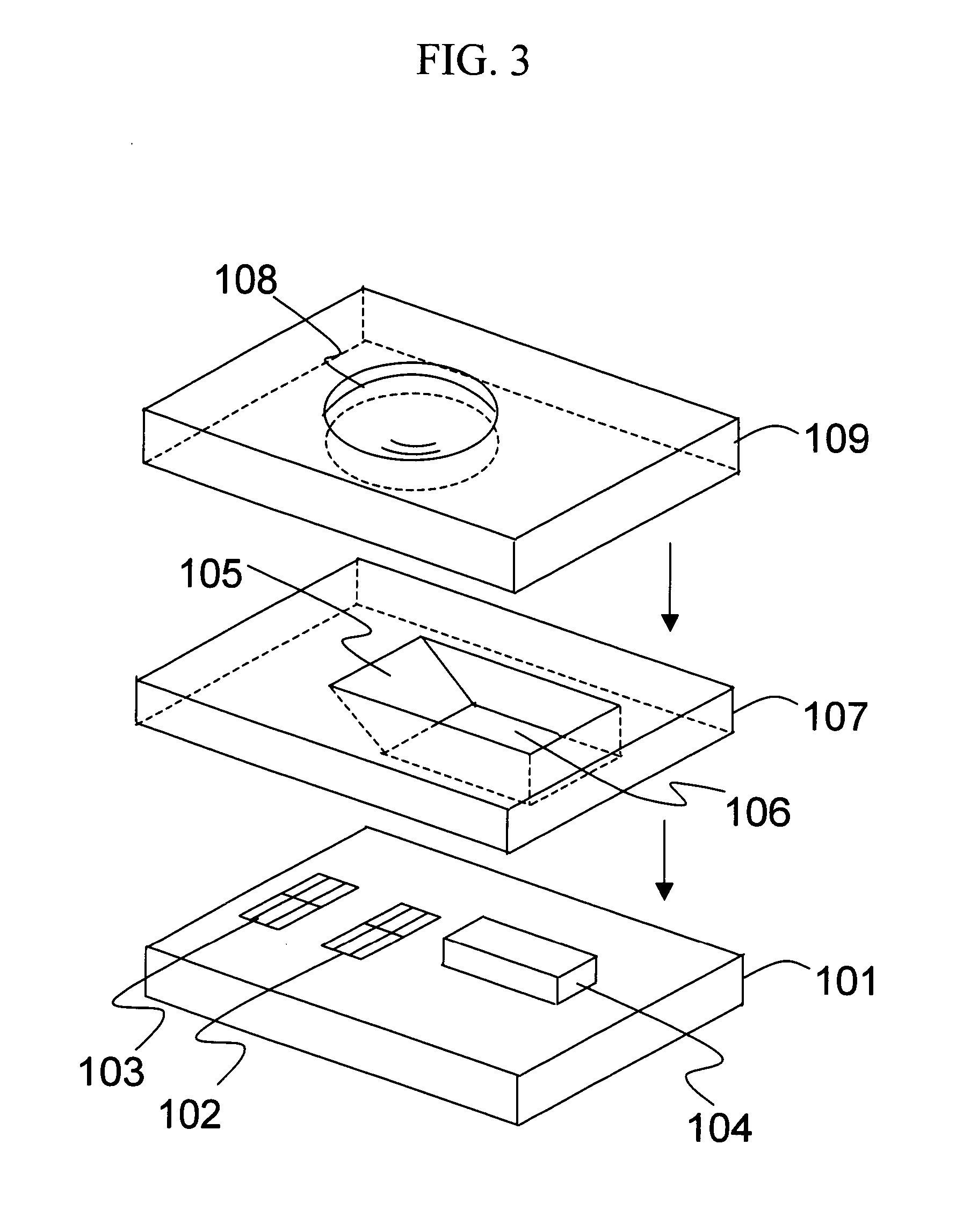
[0051]FIG. 1 shows the basic structure of an optical head according to the invention. The optical head comprises a silicon substrate 101 on which photodetectors 102 and 103 are fabricated and further a semiconductor laser 104 of the Fabry-Perot type is mounted. On top of the silicon substrate, a prism / mirror substrate 107 with a cavity 106 having a reflecting mirror 105 is bonded. On top of the prism / mirror substrate, there is further bonded a lens substrate 109 with an objective lens 108 fabricated therein. The four sides of the individual substrates are aligned such that each side is substantially in the same plane. By “substantially in the same plane” herein is meant that the plane may include some surface irregularities that are produced in practice when such layered substrate wafers are diced in a manufacturing process, as will be described later.

[0052]FIG. 2 shows a lateral cross section of the optical head shown in FIG. 1, additionally showing a light flux 201 and an optical...

embodiment 2

[0061]FIG. 8 shows a second embodiment of the invention. Light emitted by a semiconductor laser 104 is reflected by a reflecting mirror 105 and then turned into parallel beams by a collimator lens 802. The beams are then focused by an infinity objective lens 804 on a recording film on an optical information storage medium 202 through a cover layer 204 with a thickness of 0.1 mm. The semiconductor laser 104 is mounted on a radiating stem 801 made of SiC. The collimator lens 802 is comprised of an aspherical surface formed on either side of a collimator lens substrate 803. In order to reduce the distance between the end of the semiconductor laser 104 and the collimator lens 802 as much as possible while maintaining a constant focal distance, the collimator lens 802 has a meniscus shape. The objective lens 804 is an aspherical lens formed on either side of the objective lens substrate805 with an effective pupil diameter of 0.5 nun and NA of 0.85. The side of the objective lens 804 towa...

embodiment 3

[0070]FIGS. 17A and 17B show an embodiment of a small-sized optical disc unit utilizing a ultra-small optical head 1701 according to the invention. FIG. 17A is a plan view, and FIG. 17B is a side view. The small optical head 1701 is mounted on an actuator arm 1708, which can be moved finely by a focus actuator 1707 in the direction of the optical axis of the objective lens in the optical head. The actuator arm 1708 and the focus actuator 1707 are fixed to a swing arm 1703, together with a counter balance 1705. The swing arm 1703 is driven by a swing motor 1704 so as to move the small optical head 1701 in the radius direction of an optical disc 1709. The optical disc 1709 is rotated by a spindle motor 1702. Input and output of signal to the optical head are enabled by flexible plastic cables (not shown) connected to a control circuit 1706.

[0071] When the thus prepared optical head is mounted and driven on an actuator, a large amount of disc eccentricity can be dealt with even when t...


PUM

PropertyMeasurementUnit
thicknessaaaaaaaaaa
pupil diameteraaaaaaaaaa
thicknessaaaaaaaaaa

Abstract

In an optical head, if a lens is reduced in size so that it can be integrated with a light source and a photodetector, other optical components as well as the lens must be reduced in size, which would result in greater difficulties in handling for assembly and adjustment purposes. The invention allows large quantities of ultra-small optical heads to be produced accurately and at low cost, the optical heads being easy to adjust and not requiring the handling of minute components for adjustment purposes. A first substrate includes lenses for focusing light on an information storage medium, a second substrate includes detectors and disposed on the surface thereof, and a layer, which is disposed between the first and second substrates, includes prisms and mirrors. The layer also includes cavities in which light sources are disposed. The individual substrates are formed in the form of wafers with the lenses, mirrors, prisms, light sources, and photodetectors disposed thereon.

Description

CLAIM OF PRIORITY [0001] The present application claims priority from Japanese application JP 2005-052252 filed on Feb. 28, 2005, the content of which is hereby incorporated by reference into this application. BACKGROUND OF THE INVENTION [0002] 1. Field of the Invention [0003] The present invention relates to an optical head for reproducing or recording information on optical information storage media, an apparatus for reproducing and / or recording optical information, and their manufacturing method. [0004] 2. Background Art [0005] Optical disc units for CDs and DVDs are widely available examples of optical information reproducing apparatuses. In CDs, light with the wavelength of 780 nm is focused beyond a 1.2-mm thick substrate by an optical head with the numerical aperture (NA) of 0.45. In DVDs, the wavelength is reduced to 650 nm, and the NA is increased to 0.6 so as to achieve higher capacities than CDs. As a result, the thickness of the substrate of the DVD is set to be 0.6 mm i...

Claims


Application Information

Patent Timeline
Patent Type & Authority Applications(United States)
IPC IPC(8): G11B7/00
CPCG11B7/08576G11B7/1205G11B7/1374G11B7/123G11B7/22
Inventor SHIMANO, TAKESHIKANAMARU, MASATOSHIHORINO, MASAYA
Owner HITACHI LTD
Why Eureka
Try Eureka