Increasing the memory performance of flash memory devices by writing sectors simultaneously to multiple flash memory devices

a technology of flash memory and memory performance, applied in the field of digital systems, can solve problems such as affecting the overall performance of the system, and achieve the effect of increasing the performance of a digital system and reducing the time associated

Inactive Publication Date: 2006-08-31
MICRON TECH INC
View PDF99 Cites 68 Cited by
  • Summary
  • Abstract
  • Description
  • Claims
  • Application Information

AI Technical Summary

Benefits of technology

[0016] It is an object of the present invention to increase the performance of a digital system having a controller coupled to a host for operating a nonvolatile memory bank including one or more nonvolatile memory devices, such as flash and / or EEPROM chips, by reducing the time associated with reading and writing information to the nonvolatile memory bank.
[0017] It is another object of the present invention, as described herein, to decrease the time associated with storing sectors of information by writing at least two sectors of information to at least two nonvolatile memory semiconductor devices during a single write command initiated by the host.
[0018] It is another object of the present invention as described herein to decrease the time associated with reading sectors of information by reading at least two sectors of information from at least two nonvolatile memory semiconductor devices during a single read command initiated by the host.
[0020] It is yet another object of the present invention to simultaneously access two bytes of a sector of information stored within two nonvolatile memory devices thereby increasing the rate of performance of a system employing the present invention by an order of magnitude of at least two.
[0021] It is yet another object of the present invention to access one byte of a first sector and one byte of a second sector of information simultaneously within two nonvolatile memory devices thereby increasing the rate of performance of a system employing the present invention.
[0022] It is a further object of the present invention to reduce the size of a volatile memory table, or map, that maintains translations between the host-provided sector addresses to addresses of blocks within the nonvolatile memory devices thereby reducing the cost of manufacturing the digital system.

Problems solved by technology

The problem with such prior art systems is that while two bytes of information are written and read at a time, only one sector of information is accommodated at a time by the memory bank 16 during a write command initiated by the host 14.
An important problem with the prior art architecture of FIG. 2 is that while a total of 528 bytes may be stored in the I / O register 36, only one byte of sector information may be transferred at a time between the controller and the memory bank thereby impeding the overall performance of the system.

Method used


Image

  • Increasing the memory performance of flash memory devices by writing sectors simultaneously to multiple flash memory devices
  • Increasing the memory performance of flash memory devices by writing sectors simultaneously to multiple flash memory devices
  • Increasing the memory performance of flash memory devices by writing sectors simultaneously to multiple flash memory devices

Examples


Embodiment Construction

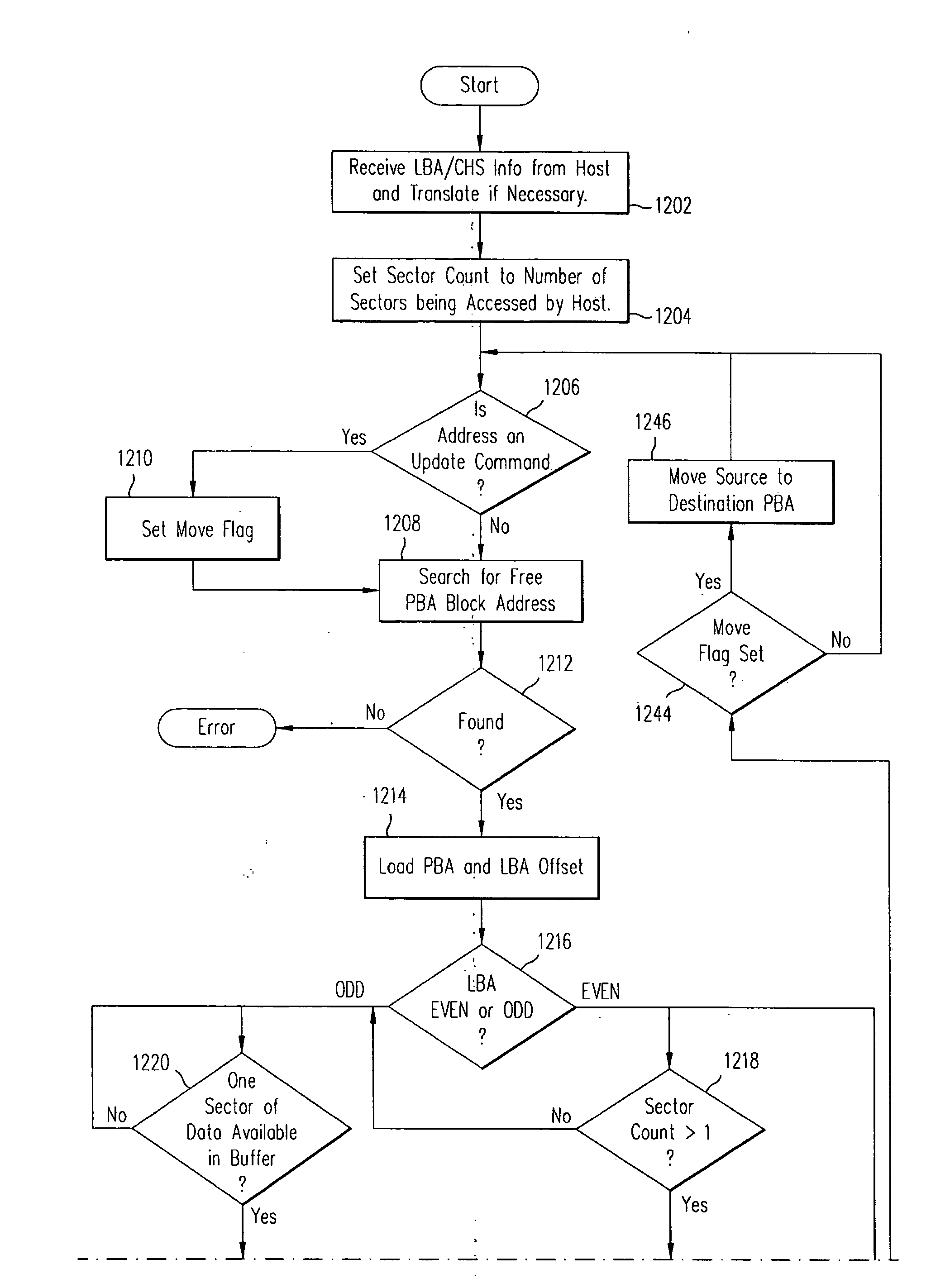
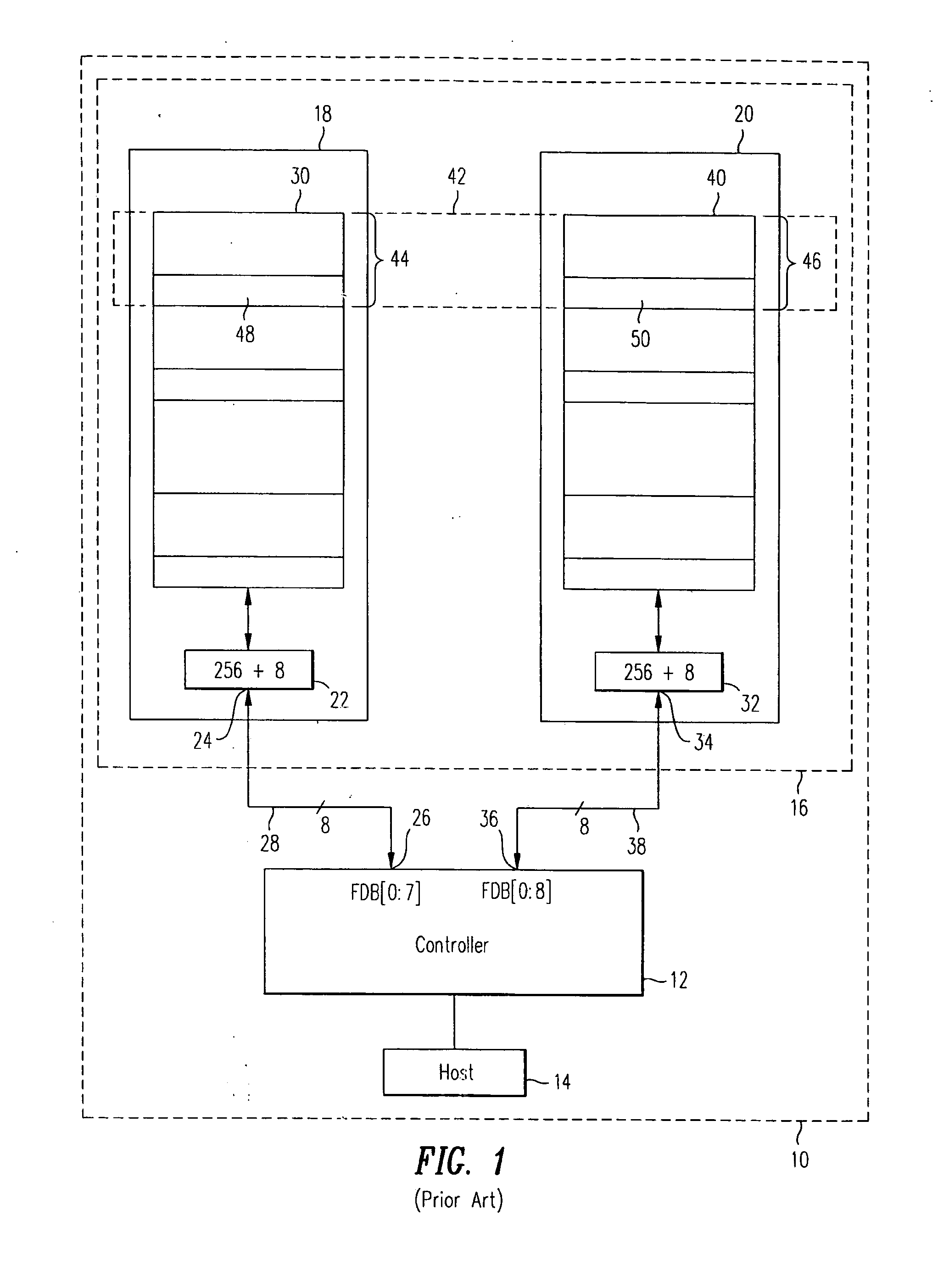
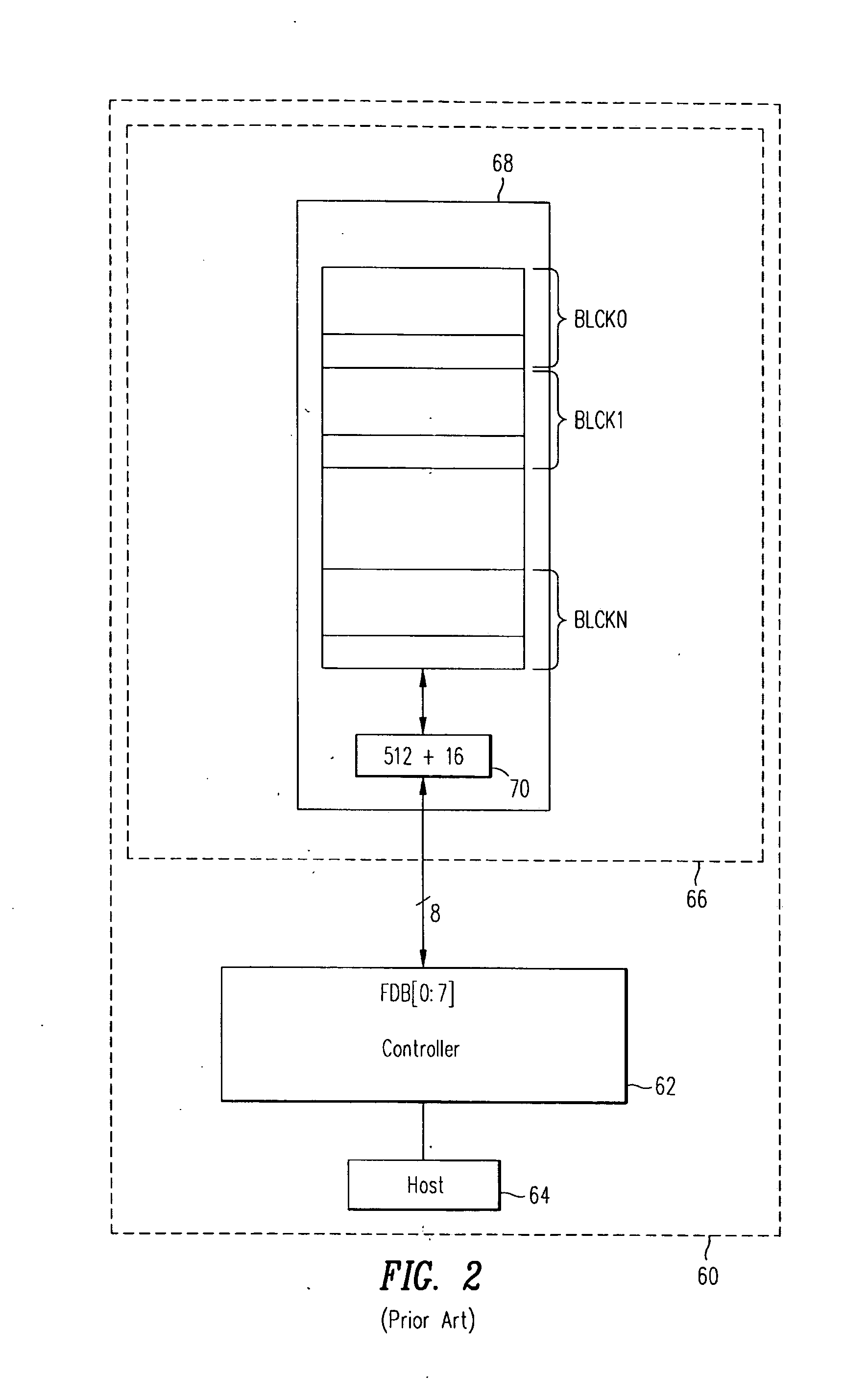
[0042]FIG. 5 shows a-generalized block diagram at 500 of a memory system in accordance with principles of the present invention. The system includes a memory card 502 coupled to a host system 504. In one embodiment, host 504 is a digital camera and memory card 502 is a digital film card, and in another embodiment, host 504 is a personal computer system and memory card 502 is a PCMCIA card. Memory card 502 includes: a non-volatile memory bank 506 including a plurality of non-volatile memory units 508 for storing sectors of information organized in blocks; a memory controller 510 coupled to the memory bank via a memory bus 512, and coupled to the host 504-via a host bus 514. Memory controller 510 controls transfer of sector-organized information between host 504 and memory bank 506. Each sector of information includes a user data portion and an overhead portion. The memory controller performs write and read operations, in accordance with the present invention, to and from the memory u...


PUM


Abstract

In one embodiment of the present invention, a memory storage system for storing information organized in sectors within a nonvolatile memory bank is disclosed. The memory bank is defined by sector storage locations spanning across one or more rows of a nonvolatile memory device, each the sector including a user data portion and an overhead portion. The sectors being organized into blocks with each sector identified by a host provided logical block address (LBA). Each block is identified by a modified LBA derived from the host-provided LBA and said virtual PBA, said host-provided LBA being received by the storage device from the host for identifying a sector of information to be accessed, the actual PBA developed by said storage device for identifying a free location within said memory bank wherein said accessed sector is to be stored. The storage system includes a memory controller coupled to the host; and a nonvolatile memory bank coupled to the memory controller via a memory bus, the memory bank being included in a non-volatile semiconductor memory unit, the memory bank has storage blocks each of which includes a first row-portion located in said memory unit, and a corresponding second row-portion located in each of the memory unit, each of the memory row-portions provides storage space for two of said sectors, wherein the speed of performing write operations is increased by writing sector information to the memory unit simultaneously.

Description

CROSS REFERENCE TO RELATED APPLICATIONS [0001] This application is a continuation of our co-pending U.S. patent application Ser. No. 10 / 832,421 filed on Apr. 26, 2004, entitled “Increasing the Memory Performance of Flash Memory Devices by Writing Sectors Simultaneously to Multiple Flash Memory Devices”, which is a continuation of our prior U.S. Pat. No. 6,728,851, issued on Apr. 27, 2004, entitled “Increasing the Memory Performance of Flash Memory Devices by Writing Sectors Simultaneously to Multiple Flash Memory Devices”, which is continuation of our prior U.S. Pat. No. 6,757,800, issued on Jun. 29, 2004, and entitled “Increasing the Memory Performance of Flash Memory Devices by Writing Sectors Simultaneously to Multiple Flash Memory Devices”, which is a continuation of our prior co-pending U.S. Pat. No. 6,397,314, issued on May 28, 2002 and entitled “Increasing the Memory Performance of Flash Memory Devices by Writing Sectors Simultaneously to Multiple Flash Memory Devices”, which...

Claims


Application Information

Patent Timeline
Patent Type & Authority Applications(United States)
IPC IPC(8): G06F12/00G06F3/06G06F11/10G06F12/02G11C16/08G11C16/10G11C29/00
CPCG06F3/0613G06F3/064G06F3/0679G06F11/1068G06F12/0238G11C16/08G11C16/102G11C29/765G11C29/82G06F12/0246
Inventor ESTAKHRI, PETROIMAN, BERHANU
Owner MICRON TECH INC
Why Eureka
Try Eureka