On-chip signal waveform measurement apparatus for measuring signal waveforms at detection points on IC chip

Inactive Publication Date: 2006-09-07
SEMICON TECH ACADEMIC RES CENT
View PDF5 Cites 44 Cited by
  • Summary
  • Abstract
  • Description
  • Claims
  • Application Information

AI Technical Summary

Benefits of technology

[0076] (1) The respective signal probing front-end circuits 30 are arranged near the corresponding detection points 33, respectively, and the signal waveform acquisition kernel circuit 90 is shared among the probing front-end circuit 30. Therefore, it is possible to reduce the effective area of the LSI chip.
[0077] (2) The digitalization function (or A/D conversion function) is mounted on each of the signal probing front-end circuits 30. This leads to that the deterioration in precision due to the multi-channeling can be suppressed.
[0078] (3) By integrating generation of analog signals on single LSI chip, the digital LSI tester can diagnose the operation of the mixed signal system LSI.
[0079] (4) Mounting of the data processing unit 40 (consisting of a counter circuit 41 and a shift register circuit 42), that repeatedly outputs judgment output probabilities Pcmp from the comparators 34 of the signal probing front-end circuits 30 at intervals of certain numbers of clocks, leads to remarkable reduction in the signal acquisition time.
[0080] (5) The on-chip waveform acquisition mechanism of the on-chip signal waveform monitoring apparatus 102 according to the f

Problems solved by technology

However, since such an LSI is configured so that many functional circuits are integrated on the LSI chip, the operation states of respective functional circuits cannot be observed from an outside of the chip.
As a result, it is difficult to perform a fault analysis in a case of an operation fault.
However, this technique has the following problems.
If only the probing front-end circuit is mounted on an LSI chip, the number of pins required for measurement becomes l

Method used


Image

  • On-chip signal waveform measurement apparatus for measuring signal waveforms at detection points on IC chip
  • On-chip signal waveform measurement apparatus for measuring signal waveforms at detection points on IC chip
  • On-chip signal waveform measurement apparatus for measuring signal waveforms at detection points on IC chip

Examples


first preferred embodiment

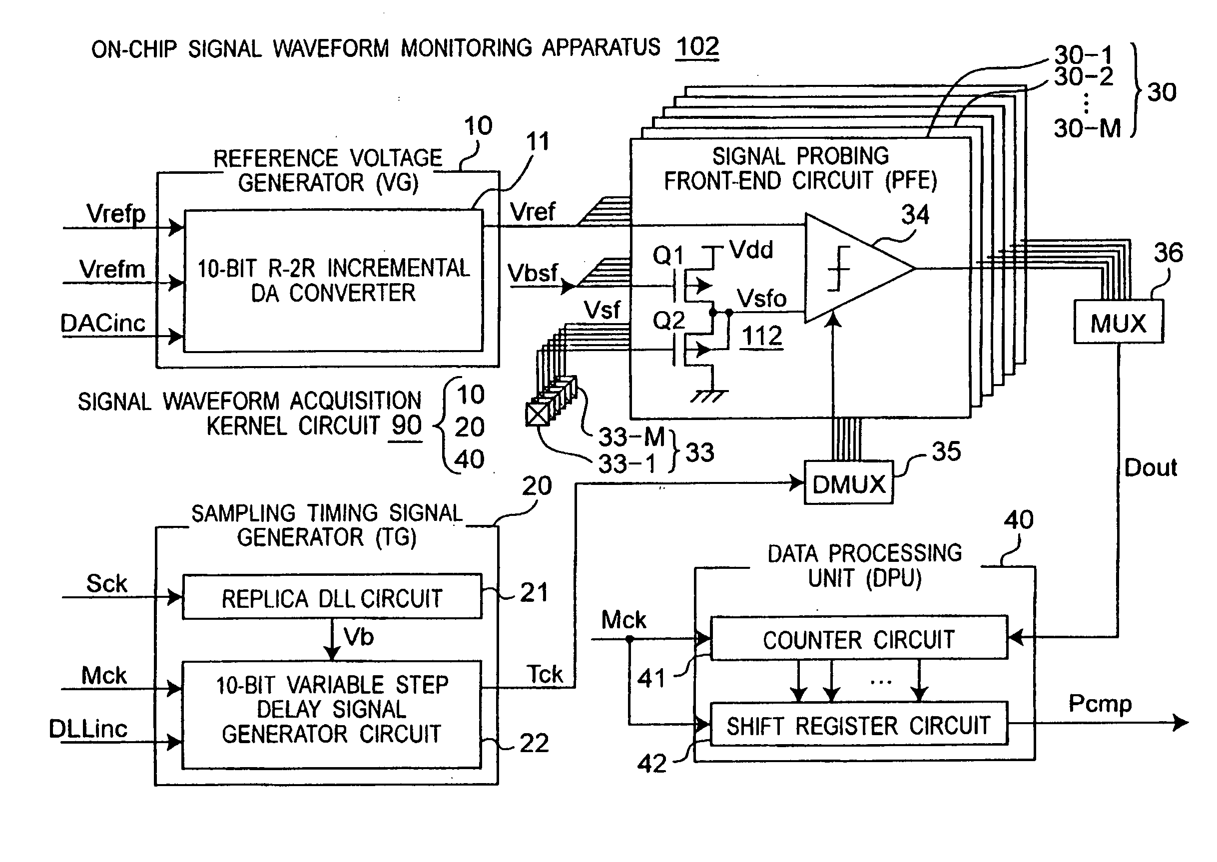
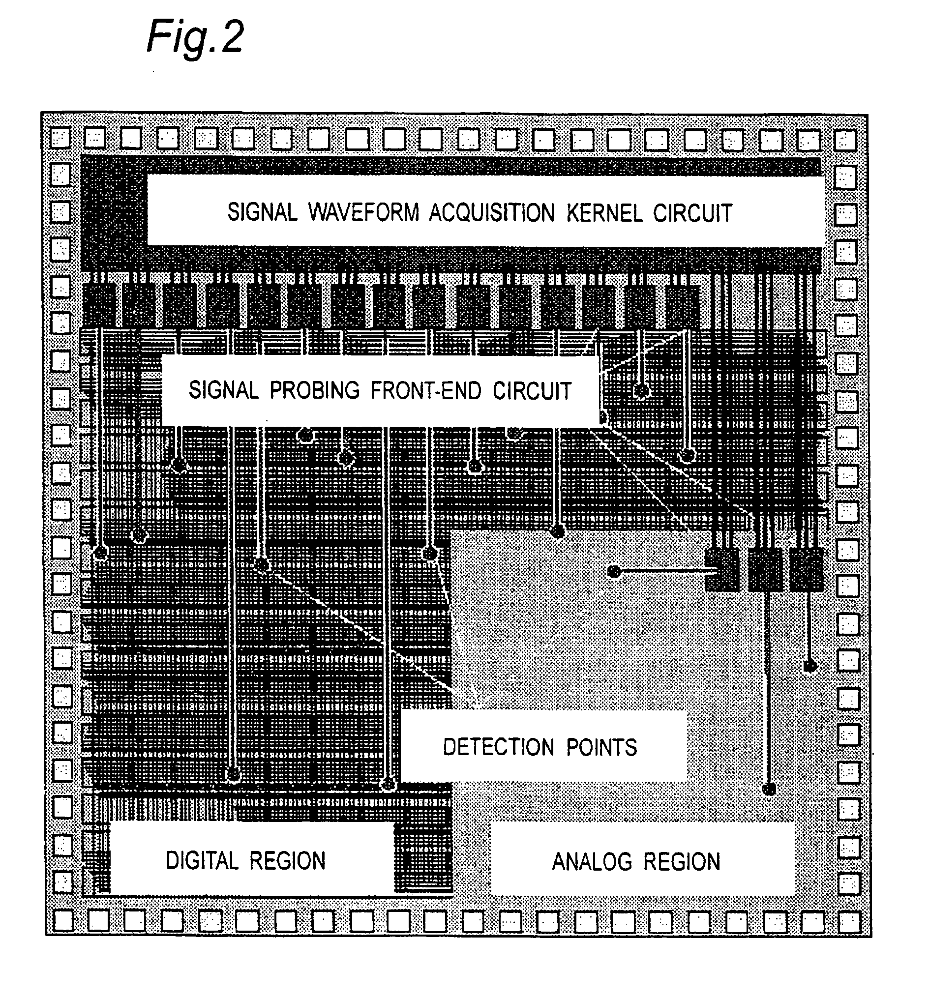
[0070]FIG. 1 is a block diagram showing a configuration of an on-chip signal waveform monitoring apparatus 102 according to a first preferred embodiment of the present invention. FIG. 2 is a plan view showing a floor plan of a system LSI, on which the on-chip signal waveform monitoring apparatus shown in FIG. 1 is mounted.

[0071] Referring to FIG. 1, the on-chip signal waveform monitoring apparatus 102 includes signal probing front-end circuits (PFE) including M signal probing front-ends 30-1 to 30-M (generically denoted by numerical reference 30), a reference voltage generator (VG) 10, a sampling timing signal generator (TG) 20, and a data processing unit (DPU) 40, and is mounted on a single LSI chip. In FIG. 2, the three circuits 10, 20, and 40 are generically referred to as a signal waveform acquisition kernel circuit 90.

[0072] In this case, the signal probing front-end circuits 30 include not only a function of detecting a signal under test at M detection points 33-1 to 33-M (g...

second preferred embodiment

[0149]FIG. 22 is a graph showing a judgment output probability Pcmp of a latch comparator 34 relative to a reference voltage Vref used in a signal waveform measurement system according to a second preferred embodiment of the present invention. FIG. 23 is a block diagram showing a configuration of the signal waveform measurement system according to the second preferred embodiment of the present invention. FIG. 24 is a block diagram showing a detailed configuration of a personal computer 200 and an FPGA 170 shown in FIG. 23.

[0150] The signal waveform measurement system according to the second preferred embodiment is characterized by sharing the functions of the data processing unit 40 according to the first preferred embodiment shown in FIG. 1 between an on-chip DPU 40A on an LSI chip and an off-chip DPU 214 of an FPGA 170 different from the LSI chip. In other words, the second preferred embodiment is characterized as follows. Functions of a decision processing for deciding the detec...

third preferred embodiment

[0176]FIG. 31 is a circuit diagram showing a configuration of a signal probing front-end circuit 30A according to a third preferred embodiment of the present invention. Namely, FIG. 31 shows the configuration of the signal probing front-end circuit 30A that employs a current mode sample hold circuit 253. The signal probing front-end circuit 30A is configured to include the following components:

[0177] (a) a source follower circuit 251 that detects a measurement target voltage Vin;

[0178] (b) a voltage-to-current converter 252 that converts the detected voltage into a current;

[0179] (c) a current mode sample hold circuit 253 that holds the current converted from the detected voltage in a holding capacitor 253C via a switch SW 21, and outputs the held current; and

[0180] (d) a current generator 254 that generates an output current lout having a predetermined magnitude proportional and corresponding to the current outputted from the sample hold circuit 253 based on the current, and ou...


PUM


Abstract

An on-chip signal waveform measurement apparatus mounted on an IC chip measures signal waveforms at detection points on the IC chip. A reference voltage generator successively generates reference voltages different from each other based on a predetermined timing signal, and Signal probing front-end circuits are mounted to correspond to the detection points, respectively, and each buffer-amplifies a voltage at each detection point, compares the buffer-amplified voltage with each reference voltage, and digitizes a comparison result into a binary digital output signal. A multiplexer time-division-multiplexes the binary digital output signals from the signal probing front-end circuits. A data processing unit calculates a judgment output probability for a detected voltage at each detection point detected by the respective signal probing front-end circuits, by counting a number of times of a predetermined binary value of the multiplexed binary digital output signal.

Description

BACKGROUND OF THE INVENTION [0001] 1. Field of the Invention [0002] The present invention relates to an on-ship signal waveform measurement apparatus for, on multi-channels, measuring signal waveforms at detection points on fixed voltage wiring lines such as internal signals, power source voltages, ground voltages, well voltages, and substrate voltages of a semiconductor large-scale integrated circuit (LSI), and a signal waveform measuring system including the on-ship signal waveform measurement apparatus. The present invention further relates to a sampling timing signal generator for use in the signal waveform measurement system. [0003] 2. Description of the Related Art [0004] With an increased degree of micro-fabrication in the semiconductor wafer fabrication process, the scale of the circuits mounted on LSI chips becomes larger. In recent years, a mixed signal system LSI in which different types of signal processing functions such as an analog processing and a digital processing ...

Claims


Application Information

Patent Timeline
IPC IPC(8): G01S13/00
CPCG01R31/2884G01R31/31924
Inventor NAGATA, MAKOTO
Owner SEMICON TECH ACADEMIC RES CENT
Why Eureka
Try Eureka