Hybrid module and production method for same, and hybrid circuit device

Inactive Publication Date: 2006-09-07
SONY CORP
View PDF4 Cites 29 Cited by
  • Summary
  • Abstract
  • Description
  • Claims
  • Application Information

AI Technical Summary

Benefits of technology

[0009] The hybrid module disclosed in the above-mentioned patent document 1 or 2 is formed by mounting a plurality of components such as semiconductor chips, functional devices, etc. side by side on a base sheet supported at the base thereof and molding a resin into a substrate body on the base sheet to seal the mounted components. In this hybrid modul

Problems solved by technology

In such a hybrid module, however, the resin-molded substrate body sealing the mounted components will incur a large dimensional change because it shrinks as the resin is cured.
Thus, the substrate body will largely be warped or otherwise deformed, resulting in misalignment of connecting pads of the components with corresponding mounting lands at the circuit board and

Method used


Image

  • Hybrid module and production method for same, and hybrid circuit device
  • Hybrid module and production method for same, and hybrid circuit device
  • Hybrid module and production method for same, and hybrid circuit device

Examples


Embodiment Construction

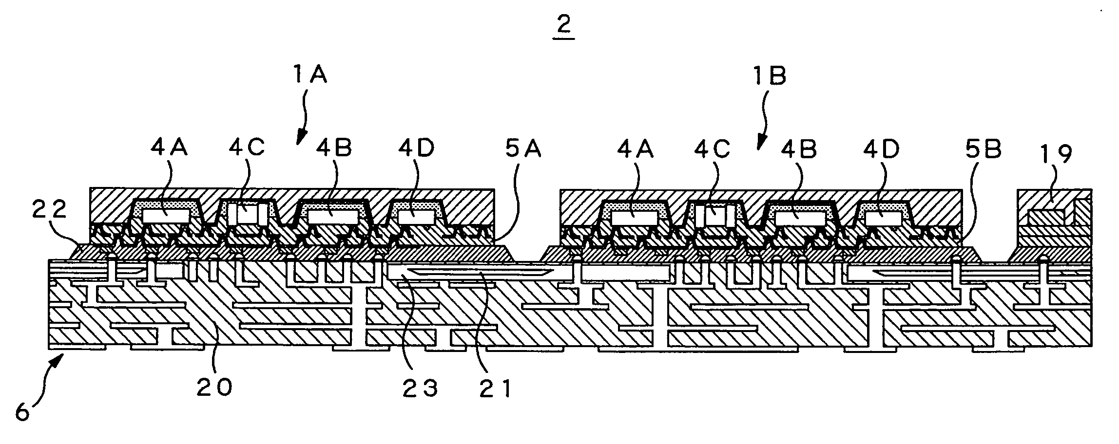
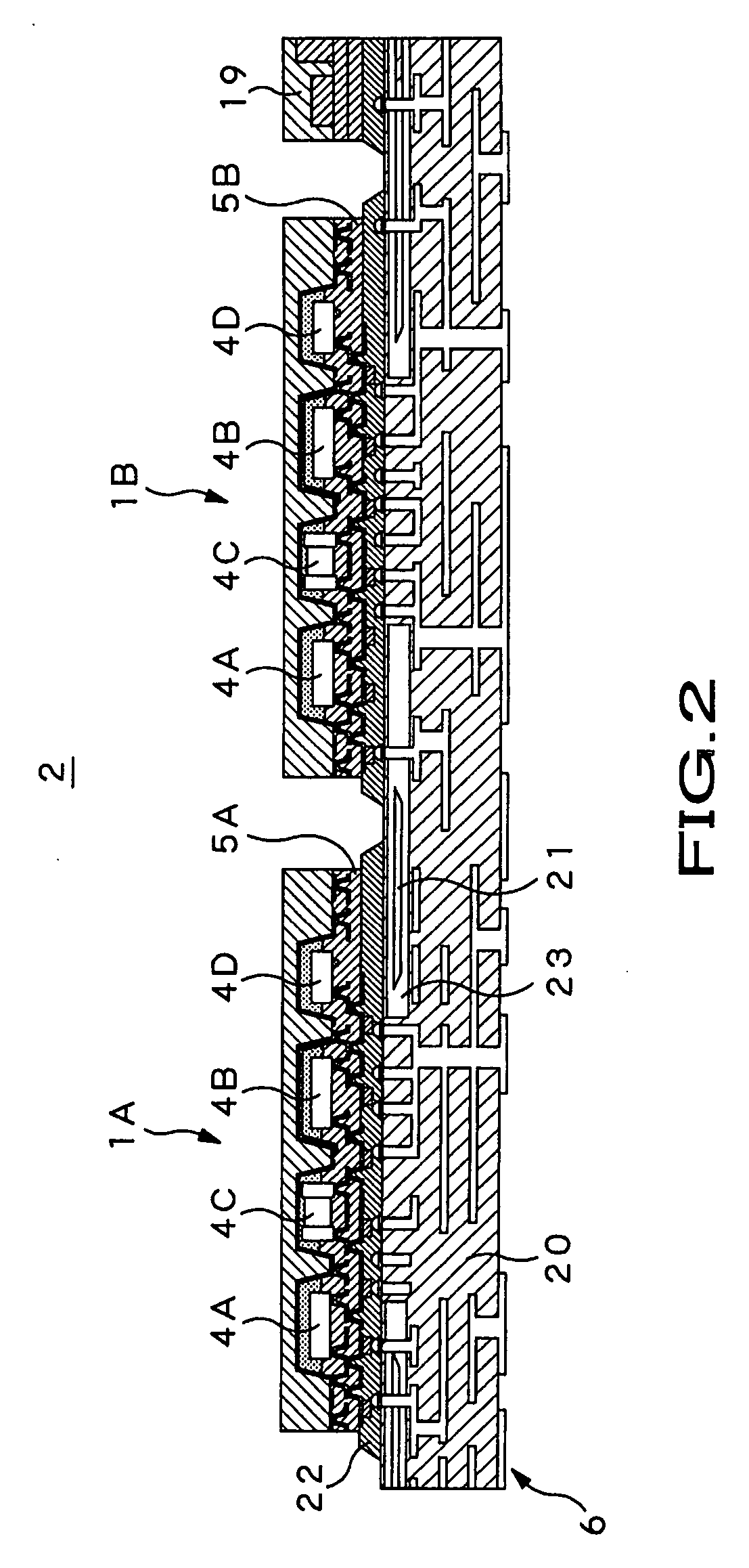
[0041] The present invention will be described in detail below concerning the embodiments thereof with reference to the accompanying drawings. FIG. 1 is a sectional view of the first embodiment of the hybrid module according to the present invention. The hybrid module is generally indicated with a reference numeral 1. As shown, the hybrid module 1 includes a silicon substrate 3, a plurality of components 4 and a wiring layer 5. FIG. 2 is a sectional view of the first embodiment of the hybrid circuit device according to the present invention. The hybrid circuit device is generally indicated with a reference numeral 2. As shown, the hybrid circuit device 2 includes two hybrid modules 1A and 2A mounted on a base substrate 6. The hybrid circuit device 2 is used in, for example, a personal computer, mobile phone and other electronic devices to perform an electric wiring function for transmission and reception of electric control signals and data signals and for supplying a power as well ...


PUM


Abstract

Components can be mounted with an improved accuracy and efficiency, thereby realizing a thin hybrid module in which the components are mounted with a high density. The present invention provides a hybrid module including a silicon substrate having formed therein a plurality of component mounting concavities open to one of main sides of the silicon substrate, a plurality of components inserted in the component mounting concavities, respectively, with their input/output-formed sides being exposed to outside through the openings of the component mounting concavities and buried in the silicon substrate with their perimeters except for at least their input/output-formed sides being fixed by adhesive layers formed in the component mounting concavities, and a wiring layer formed on the main side of the silicon substrate to cover the components and which has a wiring pattern provided on an insulative resin layer included in the wiring layer and which is connected to an input/output provided on the input/output-formed side of each of the components.

Description

CROSS REFERENCES TO RELATED APPLICATIONS [0001] The present invention contains subject matter related to Japanese Patent Application JP 2005-054842 filed in the Japanese Patent Office on Feb. 28, 2005, the entire content of which is incorporated herein by reference. BACKGROUND OF THE INVENTION [0002] 1. Field of the Invention [0003] The present invention relates to a hybrid module having a plurality of components such as chips, IC (integrated circuit) elements or optical elements installed on a silicon substrate and including a wiring layer and a production method for the hybrid module, and a hybrid circuit device having the hybrid module installed thereon. [0004] 2. Description of the Related Art [0005] For example, various electronic devices such as a personal computer, mobile phone, video recorder or audio device use various semiconductor circuit elements and electronic components such as IC (integrated circuit) elements, LSI (large-scale integration) elements or memory elements....

Claims


Application Information

Patent Timeline
IPC IPC(8): G02B6/12H01L33/48
CPCG02B6/12002G02B6/12004H01L2924/07802H01L2924/00014H01L2924/12041H01L2224/45147H01L24/19H01L2924/014H01L2924/01076H01L2924/01024H01L2924/01006H01L2924/01005H05K1/185H05K1/0274G02B6/4214G02B2006/12173H01L23/5385H01L23/5389H01L24/24H01L24/82H01L25/0655H01L25/167H01L31/0203H01L31/12H01L2224/24227H01L2224/82039H01L2224/83192H01L2224/92H01L2224/92244H01L2924/01002H01L2924/01004H01L2924/01029H01L2924/01033H01L2924/01078H01L2924/01079H01L2924/01082H01L2924/09701H01L2924/14H01L2924/15153H01L2924/15157H01L2924/15165H01L2924/30105H01L2224/83H01L2224/82H01L2924/00H01L2224/48H01L2924/351H01L2924/12043H01L2924/00011H01L25/04
Inventor OGAWA, TSUYOSHINAKAYAMA, HIROKAZU
Owner SONY CORP
Why Eureka
Try Eureka