
Insulator composition, organic semiconductor device, electronic device, and electronic apparatus

Inactive Publication Date: 2006-09-14
SEIKO EPSON CORP
View PDF7 Cites 15 Cited by
  • Summary
  • Abstract
  • Description
  • Claims
  • Application Information

AI Technical Summary

Benefits of technology

[0009] An advantage of the invention is to provide an insulator composition capable of easily forming an insulating section with high hygroscopicity, and an organic semiconductor device, an electronic device, and an electronic apparatus that have high reliability.
[0010] Such an advantage can be achieved according to aspects of the invention as described below.
[0011] An insulator composition according to a first aspect of the invention includes a polysilsesquioxane derivative with an organic group as a substituent, and is used for the formation of an insulating section that an organic semiconductor device includes.
[0012] Thus, the insulating section with high hygroscopicity can easily be formed.
[0013] In the insulator composition according to the first aspect of the invention, the polysilsesquioxane derivative is preferably at least one kind of compounds represented by formulas (1) to (3)
[0014] where each R independently represents any one of an alkyl group, alkoxy group, aryl group, and aryl group in which at least one hydrogen atom is replaced by a halogen atom, and in the formula (1), n is an integer from 1 to 3.

Problems solved by technology

However, this gate insulating layer requires a vapor phase film formation method to be used for its formation, and therefore involves problems.
Its formation by using the method takes time and trouble.
Furthermore, the method may cause the deterioration or degradation of the organic semiconductor layer during the formation of the gate insulating layer.

Method used


Image

  • Insulator composition, organic semiconductor device, electronic device, and electronic apparatus
  • Insulator composition, organic semiconductor device, electronic device, and electronic apparatus
  • Insulator composition, organic semiconductor device, electronic device, and electronic apparatus

Examples


example 1

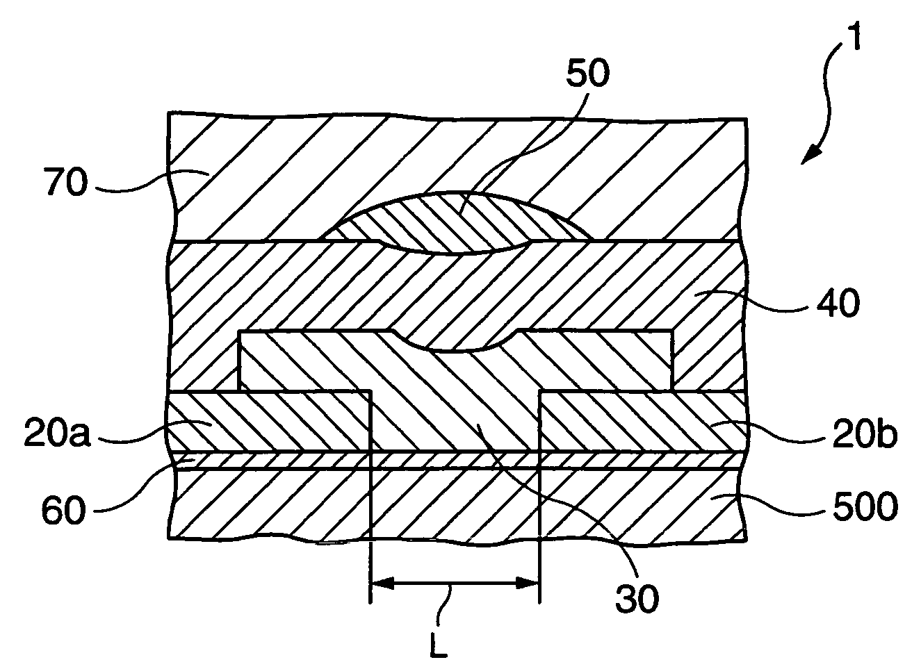
[0173] [1] A glass substrate (manufactured by NEC Corning Inc., “0A10”) was prepared, cleaned by using water, and thereafter dried.

[0174] [2] A 5% wt / vol solution of polymethyl methacrylate (PMMA) in butyl acetate was applied by a spin coating method (2400 rpm), and thereafter dried at 60° C. for 10 minutes.

[0175] Thus, a buffer layer having an average thickness of 500 nm was formed.

[0176] [3] A resist layer was formed on the buffer layer in an area other than the area for forming a source electrode and a drain electrode.

[0177] A gold thin film was formed on the buffer layer that was exposed from the resist layer by a vapor deposition method, and thereafter the resist layer was removed.

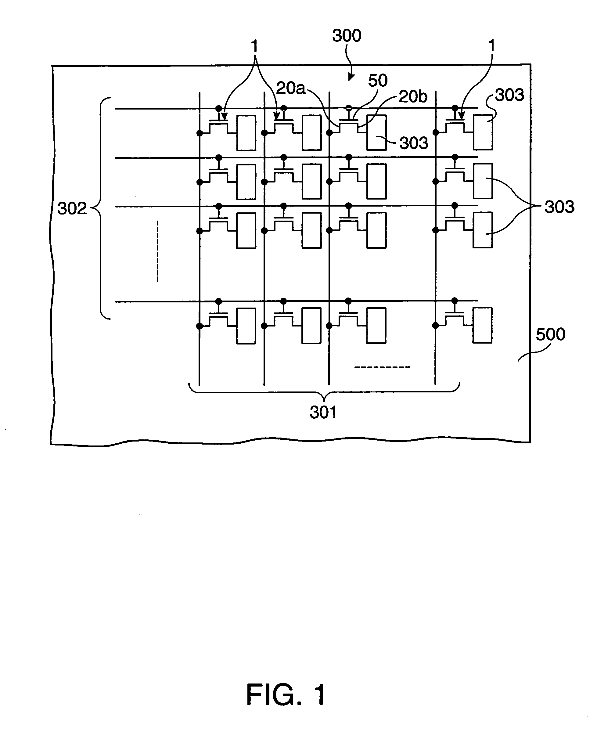
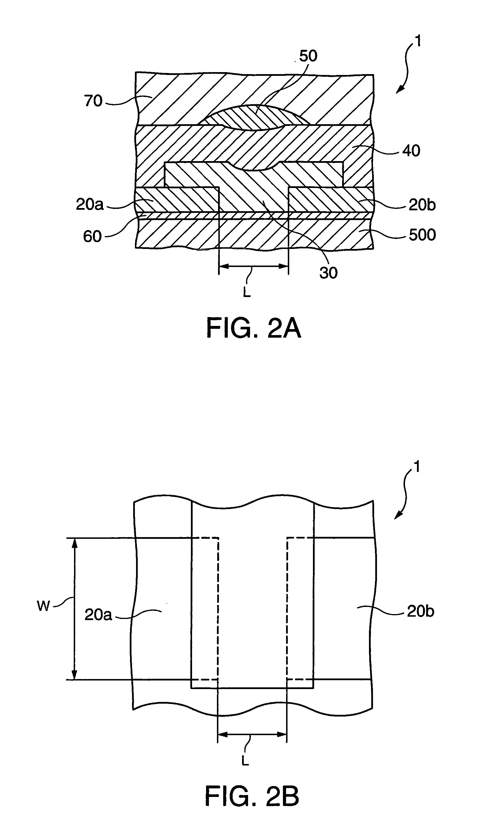
[0178] As a result, the source electrode and the drain electrode both having an average thickness of 100 nm were formed.

[0179] The distance between the source electrode and the drain electrode (channel length L) was 20 μm and the channel width W was 1 mm.

[0180] [4] A 1% wt / vol solution of fluor...

example 2

[0189] A TFT was fabricated in the same manner as in Example 1, with the exception of using the insulator composition B in the process [5] described above.

example 3

[0190] A TFT was fabricated in the same manner as in Example 1, with the exception of using the insulator composition C in the process [5] described above.


PUM

PropertyMeasurementUnit
Percent by massaaaaaaaaaa
Compositionaaaaaaaaaa
aaaaaaaaaa

Abstract

An insulator composition includes a polysilsesquioxane derivative with an organic group as a substituent, the insulator composition being used for formation of an insulating section that an organic semiconductor device includes.

Description

BACKGROUND OF THE INVENTION [0001] 1. Technical Field [0002] The present invention relates to an insulator composition, an organic semiconductor device, an electronic device, and an electronic apparatus. [0003] 2. Related Art [0004] In recent years, it has been promoted to develop thin film transistors (TFTs) using organic materials (organic semiconductor materials) that exhibit semiconducting conductivity. [0005] These TFTs have advantages such as suitability for thickness and weight reduction, flexibility, and low material cost, and therefore are expected to be used as switching elements for flexible displays and the like. [0006] Among the TFTs as described above, there is a TFT using an inorganic material as the material for its gate insulating layer. For reference, see JP-A-2000-103719, which is an example of related art. [0007] If a gate insulating layer is made by using an inorganic material, the gate insulating layer prevents the invasion of moisture into an organic semicondu...

Claims


Application Information

Patent Timeline
IPC IPC(8): H01L29/94
CPCC08K5/5435C08K5/549H01B3/46H01L51/0036H01L51/0039H01L51/0043H01L51/052H10K85/115H10K85/151H10K85/113H10K10/471
Inventor YAMAMOTO, HITOSHIMORIYA, SOICHI
Owner SEIKO EPSON CORP
Learn More