Method of manufacturing vibrating micromechanical structures

a micromechanical structure and vibrating technology, applied in the direction of microstructural system formation, electrical transducer, conductive pattern formation, etc., can solve the problems of low yield, low yield, and difficult control of intrinsic stresses and stress gradients

Inactive Publication Date: 2006-09-21
HONEYWELL INT INC
View PDF19 Cites 219 Cited by
  • Summary
  • Abstract
  • Description
  • Claims
  • Application Information

AI Technical Summary

Benefits of technology

[0037] According to other aspects of the invention, an improved micromechanical resonator structured of single crystal silicon wafer material is provided using the method of the present invention.

Problems solved by technology

These intrinsic stresses and stress gradients are difficult to control during manufacturing.
This state of the art method of manufacturing using polysilicon also requires removal of a sacrificial layer of material using wet etching techniques that complicate the manufacturing process and generally results in low yield due to difficulty in removing sacrificial material in the small gap between the resonator and the lower electrode.
This method of manufacturing using polycrystalline silicon also results in stiction, which further lowers yields.
For devices requiring very small capacitive air gaps, e.g., to compensate for manufacturing tolerances or for tuning or for use as tunable resonator cum filter, the removal of sacrificial layer becomes extremely difficult as liquid or even vapor etching techniques cannot easily penetrate underneath the resonators to create a free standing structures.
Additionally, impurities present in polysilicon thin films degrade device performance and also result in lower resonator Q.
Additionally, cleaning and removal of the sacrificial layer is extremely difficult for small gaps, and often requires use of a surfactant.
These state of the art methods of manufacturing using polycrystalline silicon also require removal of a sacrificial layer of material using wet etching techniques that complicate the manufacturing process and generally results in low yield due to difficulty in removing sacrificial material in the small gap between the resonator and the lower electrode.
This method of manufacturing using polycrystalline silicon also results in stiction, which further lowers yields, and impurities present in polysilicon thin films degrade device performance and result in lower resonator Q.

Method used


Image

  • Method of manufacturing vibrating micromechanical structures
  • Method of manufacturing vibrating micromechanical structures
  • Method of manufacturing vibrating micromechanical structures

Examples


Embodiment Construction

[0051] In the Figures, like numerals indicate like elements.

[0052] The present invention is an apparatus and method for fabrication of micromechanical resonators using a two-wafer process, including a Silicon-on-Insulator (SOI) base wafer and a SOI resonator wafer, or alternatively an insulating base wafer and a single crystal silicon (SCS) or SOI resonator wafer.

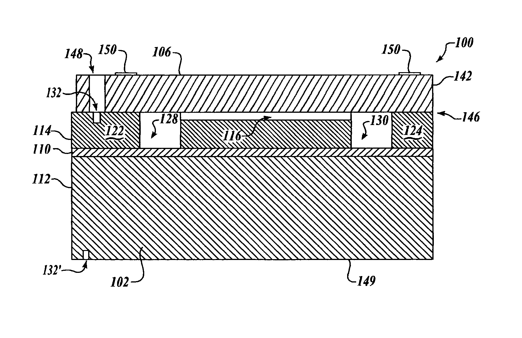
[0053]FIG. 7 is a cross-sectional view that illustrates the architecture of a micromechanical resonator device 100 of the present invention formed of a SOI base plate 102 formed in a SOI base wafer 104 and a single crystal silicon micromechanical resonator 106 formed in a SOI resonator wafer 108 (shown in subsequent Figures and described below). The SOI base and resonator wafers are a type that is generally commercially available. The SOI base wafer element 104 includes a buried dielectric layer 110 having a typical thickness of from about 0.5 to 2.0 microns that is sandwiched between relatively thicker “handle” and “acti...


PUM

PropertyMeasurementUnit
thicknessaaaaaaaaaa
thicknessaaaaaaaaaa
dielectricaaaaaaaaaa

Abstract

A method for fabrication of single crystal silicon micromechanical resonators using a two-wafer process, including either a Silicon-on-insulator (SOI) or insulating base and resonator wafers, wherein resonator anchors, a capacitive air gap, isolation trenches, and alignment marks are micromachined in an active layer of the base wafer; the active layer of the resonator wafer is bonded directly to the active layer of the base wafer; the handle and dielectric layers of the resonator wafer are removed; viewing windows are opened in the active layer of the resonator wafer; masking the single crystal silicon semiconductor material active layer of the resonator wafer with photoresist material; a single crystal silicon resonator is machined in the active layer of the resonator wafer using silicon dry etch micromachining technology; and the photoresist material is subsequently dry stripped.

Description

FIELD OF THE INVENTION [0001] The present invention relates to methods of fabricating micromechanical resonators using Silicon-on-insulator (SOI) wafers, and in particular to methods of fabricating micromechanical resonators using single crystal silicon wafer material. BACKGROUND OF THE INVENTION [0002] As disclosed by Yoon, et al. in U.S. Pat. No. 6,490,147, “High-Q Micromechanical Device and Method of Tuning Same,” Dec. 3, 2002, which is incorporated herein by reference, and also by Nguyen, et al. in U.S. Pat. No. 6,249,073, “Device Including a Micromechanical Resonator Having an Operating Frequency and Method of Extending Same,” Jun. 19, 2001, which is incorporated herein by reference, vibrating micromechanical resonators formed of polycrystalline silicon, commonly known as polysilicon, are well-known as miniaturized substitutes for crystals in a variety of high-Q oscillator and filtering applications. State of the art micromechanical resonator fabrication techniques utilize poly...

Claims


Application Information

Patent Timeline
Patent Type & Authority Applications(United States)
IPC IPC(8): H05K3/20H05K3/02
CPCB81B2201/0271B81C1/00142B81C2201/019B81C2203/036B81C2203/051H03H3/0072Y10T29/49156H03H9/462Y10T29/49155Y10T29/49861Y10T29/49826Y10T29/49128Y10T29/49005H03H9/2447
Inventor JAFRI, IJAZ H.KLEIN, JONATHAN L.MAGENDANZ, GALEN P.
Owner HONEYWELL INT INC
Why Eureka
Try Eureka