Tag antenna

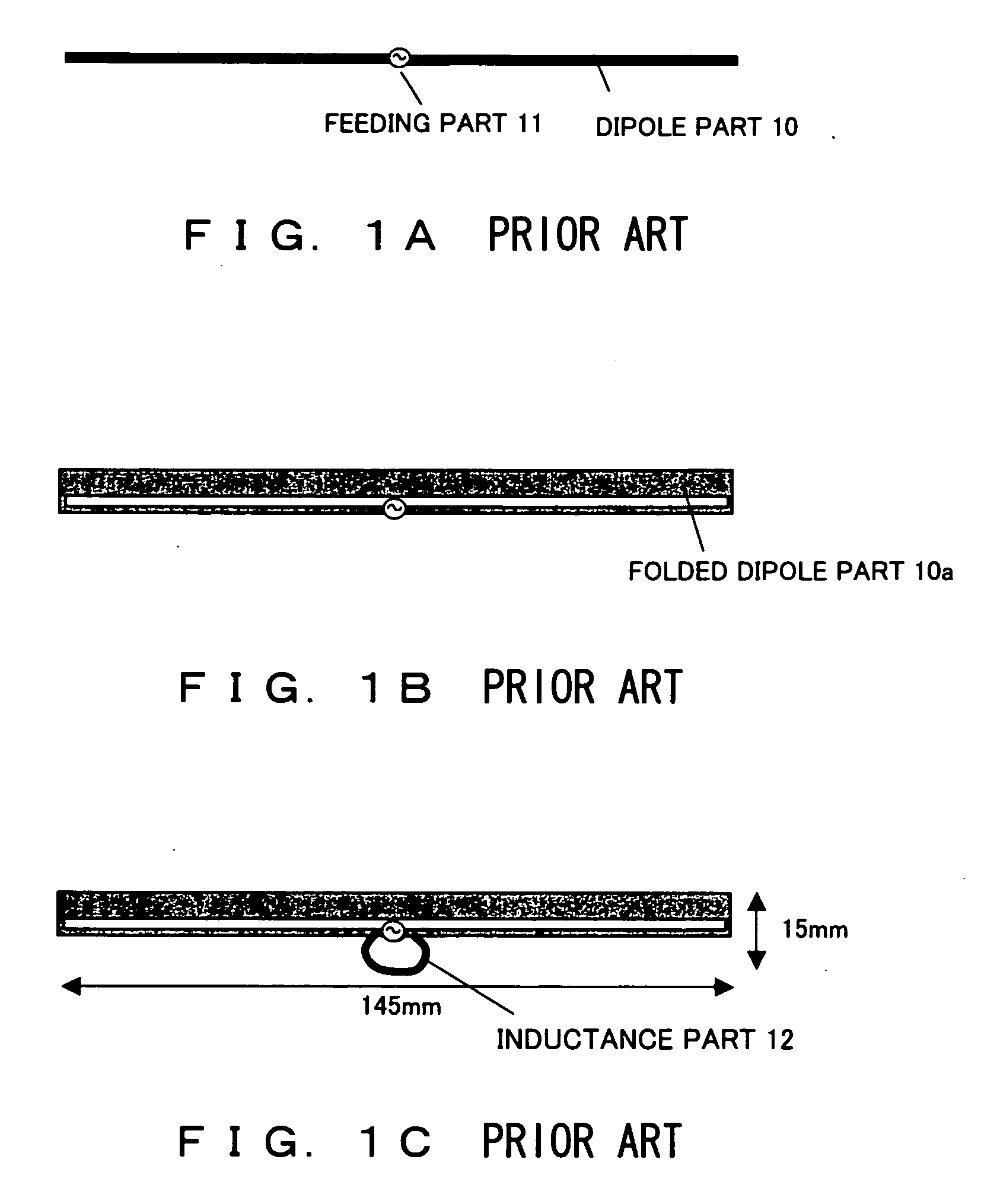
a technology of tag antenna and tag antenna, which is applied in the direction of resonant antenna, record carrier used with machines, instruments, etc., can solve the problems of impracticality, inability to meet the needs of miniaturization, and large height of 15 mm and width of 145 mm, so as to reduce the cost of the antenna

Active Publication Date: 2006-09-21
FUJITSU LTD
View PDF20 Cites 33 Cited by
  • Summary
  • Abstract
  • Description
  • Claims
  • Application Information

AI Technical Summary

Benefits of technology

[0015] A small antenna which has an antenna length smaller than λ/2 (λ being the antenna resonance wavelength) can be formed, and a communication distance which is 60 to 7...

Problems solved by technology

However, because an antenna with a height of about 15 mm and width of about 145 mm is too large and impractical, miniaturization is necessary.
However, when the antenna is miniaturized, resonance conditions do not match wit...

Method used


Image

  • Tag antenna
  • Tag antenna
  • Tag antenna

Examples


first embodiment

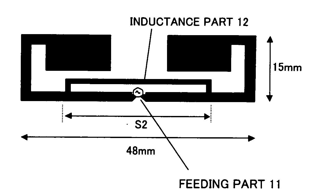
[0039]FIG. 4 to FIG. 11 are diagrams explaining the present invention.

[0040] As shown in FIG. 6, a dipole is formed with a height of 15 mm×width of 48 mm (effective total length, approximately 116 mm=⅜λ), under the constraint of an area smaller than ¼of a card area. The antenna in FIG. 3 has a rolled dipole part 10. Electromagnetic field simulation is performed for this antenna configuration, and when the calculation results of f=700 MHz to 3000 MHz are plotted on an admittance chart, a trajectory (antenna without L) such as the thin line of FIG. 4 is formed. At the imaginary part=0, f=1340 MHz, which is large, and Ra=16Ω, because the RFID tag antenna is miniaturized. Generally, if the dipole is bent, the radiation resistance Ra becomes smaller than the Ra=72Ω of an ordinary straight dipole. In this case, the f=953 MHz point is in a position shown by a triangle indicated as an antenna without L in FIG. 4. Then, by connecting an inductance part (S2=30 mm) 12 to this dipole in paralle...

second embodiment

[0046]FIG. 12A to FIG. 14 are diagrams explaining the present invention.

[0047] In RFID, the tag antenna may be implemented adhered to a target object. In this case, the most suitable inductance must be selected very carefully because the resonance wavelengths change due to the specific dielectric constant (∈r) of the object to which it is adhered.

[0048] As shown in FIG. 12A, the dipole was formed with a height of 10 mm and a width of 60 mm (effective total length, approximately 75 mm=λ / 4) and designed using electromagnetic simulation and experimental product measurements with the same considerations as the first embodiment. The thickness of the object to which the antenna is adhered is assumed to be t=1 mm and the specific dielectric constant to be εr=1, 3, or 5 (air is εr=1, plastic is εr=3 to 4, and rubber is εr=4 to 5). As a result, the inductance La of the antenna to the inductance length S2 is the value shown in FIG. 13. Because it is known from the first embodiment that the a...

third embodiment

[0053]FIG. 15 to FIG. 21 are diagrams explaining the present invention.

[0054] As shown in FIG. 15, under the assumption that the size is half of a card size, a bow-tie-shaped dipole (Bow Tie part 13) was formed with a height of 37 mm and a width of 48 mm (effective total length, approximately 110 mm=⅜λ) and designed using electromagnetic simulation and experimental product measurements with the same considerations as the first embodiment. As a result, the La value became that shown in FIG. 16 as a function of the inductance length S1. Because it is known from the first embodiment that the actual measurement and the simulation value for inductance almost match, this simulation value is reliable. In addition, from the results of the experimental production of the antenna, the antenna radiation resistance is Ra=1150Ω regardless of the S1 value. Further, the simulation value of the gain is the value shown in FIG. 14. Because the area of the dipole part is larger than that of the antenna...


PUM


Abstract

A dipole part of a length shorter than half of an antenna resonance wavelength is placed so as to be rolled and enables a feeding part 11 to feed a chip. An inductance part 12 for adjusting the inductance of the antenna is provided so as to sandwich the feeding part 11. The inductance 12 is provided using an empty space of the inside of the rolled dipole part. By providing the inductance part 12, the inductance of the antenna can be adjusted so as to resonate at a predetermined frequency with the capacitance of the chip connected to the feeding part 11. At this time, although the radiation resistance of the antenna becomes extremely large according to calculations, it is actually almost the same as the resistance of the chip due to loss, and the power received by the antenna can be provided to the chip.

Description

BACKGROUND OF THE INVENTION [0001] 1. Field of the Invention [0002] The present invention is related to a non-contact tag antenna which communicates RFID reader / writer. [0003] 2. Description of the Related Arts [0004] A system which enables a reader / writer to read information from a tag by transmitting a signal of approximately 1 W from the reader / writer, receiving this signal at the tag-end, and returning a response signal to the reader / writer, again, using the UHF band (860 to 960 MHz) radio signals, is called an RFID system. Although the communication distance thereof differs according to the tag antenna gain, chip operation voltage, and peripheral environment, it is about 3 m. A tag comprises an antenna with a thickness of 10 to 30 μm and an LSI chip which is connected to the antenna feed point. [0005]FIGS. 1A to 1C are diagrams explaining the tag antenna used in a conventional RFID system. FIG. 2 is a diagram showing an equivalent circuit of an RFID tag antenna. FIG. 3 is a dia...

Claims


Application Information

Patent Timeline
IPC IPC(8): H01Q9/28
CPCH01Q1/22H01Q1/2225H01Q9/24H01Q9/285G06K19/07773
Inventor KAI, MANABUMANIWA, TORUYAMAGAJO, TAKASHI
Owner FUJITSU LTD
Why Eureka
Try Eureka