

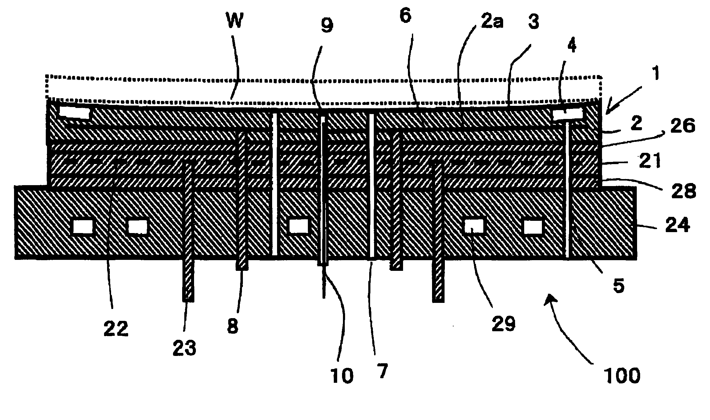
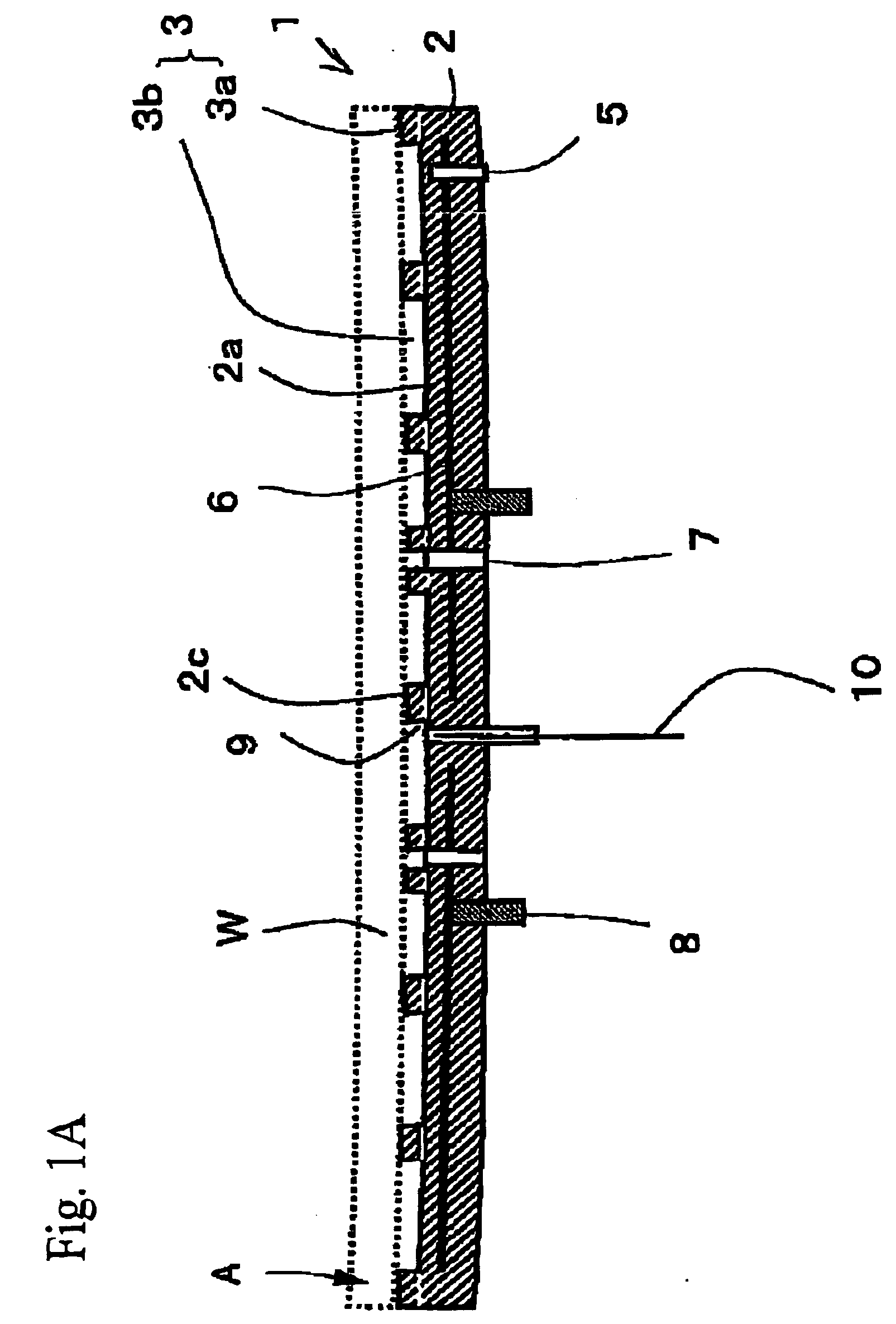
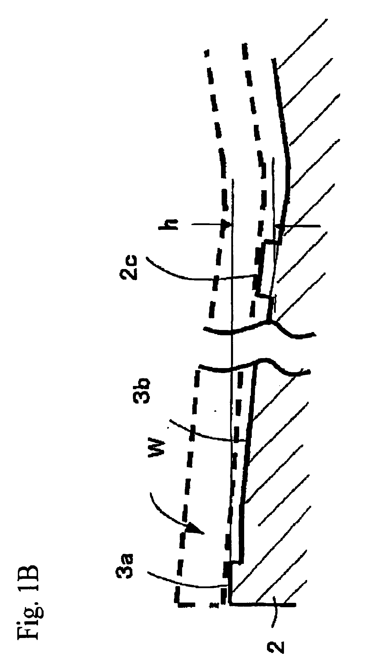
Electrostatic chuck and wafer holding member and wafer treatment method
a technology of holding member and chuck, which is applied in the direction of electrostatic charges, electrical equipment, capacitors, etc., can solve the problems of significant temperature difference in the wafer surface, deterioration of uniform heating properties, and high risk of causing a wide temperature difference in the respective surface of the wafer, so as to shorten the separation time of the wafer w, reduce the amount of gas leakage, and high attraction power
- Summary
- Abstract
- Description
- Claims
- Application Information
AI Technical Summary
Benefits of technology
Problems solved by technology
Method used
Image

Examples
example 1
[0116] An aluminum nitride powder with an average particle diameter of 1 μm and produced by a method for a reductive nitridation was used as a raw material. Further, a carbon powder with an average particle diameter of 1 μm and 10% by weight of a CeO2 powder with an average particle diameter of 1 μm were added and the resulting powder mixture was adjusted so as to suppress metals other than Al to 1% by weight or less and mixed
[0117] The mixed powder was further mixed with ethanol and a binder to obtain a powder for molding. The powder for molding was molded in a disk-like shape with a diameter of 400 mm and a thickness of 6 mm by a press molding. Further, the powder was molded into a shape with a diameter of 80 mm and a thickness of 4 mm as a sample for measurement. An electrode was formed by using a paste containing WC, AlN and an organic hinder. A pair of disks were layered while sandwiching the electrode and the pair of the disks layered in such a manner were pressed and the res...
example 2
[0126] Heat radiating sheets and cooling members were stuck to electrostatic chucks in the same manner as Example 1 and the circular projected parts were ground in the same manner by a rotary grinding machine to obtain samples No. 21 to No. 23.
[0127] With respect to the samples No. 21 and No. 22, the gas packing faces was processed to be concave faces. The center parts of the gas packing faces were lowered and the difference of the average height of 5 points in the circular projected parts was adjusted to be 10 μm.
[0128] With respect to the sample No. 23, the gas packing face was made to be flat. The height of the center part in the gas packing face was lowered and the difference of the average height of 5 points in the circular projected parts was adjusted to be 10 μm.
[0129] Further, a sample No. 24 was machined using a rotary grinding machine to adjust the height of the circular projected part of the setting face and the height of the gas packing face to be the same.
[0130] Wit...
example 3
[0134] Plate-shaped ceramic bodies were produced in the same manner as Example 1 and a metal Ti film was formed in the undersurface of each plate-shaped ceramic body to use it as an electrode for electrostatic attraction. The width of a circular projected part was set to be 1.5 mm and a circular recessed part with a width of 1 mm was formed in the inside. The electrode for the electrostatic attraction was formed to be a parabolic toothcomb-like shape and its external shape was made to be circular. Samples No. 31 to No. 33 and No. 35 to No. 37 had the size of the outer diameter of the electrode for the electrostatic attraction same as the outer diameter of the circular recessed part. Sample No. 34 had the outer diameter of the electrode for electrostatic attraction same as the inner diameter of the circular recessed part.
[0135] These Samples were individually set in the vacuum container and heated to 100° C. in the same manner as Example 1. The temperature difference in each wafer f...
PUM
 Abstract
Description
Claims
Application Information