
High-frequency distribution circuit for distributing high-frequency signal

a high-frequency distribution and high-frequency signal technology, applied in the field of high-frequency distribution circuits, can solve the problems of increasing current consumption, poor isolation, and increasing the cost of providing the lnb, sw-box or other similar products with a termination as an accessory, so as to prevent the variation in the level of the received signal and poor isolation

Inactive Publication Date: 2006-09-21
SHARP KK
View PDF4 Cites 3 Cited by
  • Summary
  • Abstract
  • Description
  • Claims
  • Application Information

AI Technical Summary

Benefits of technology

The present invention provides an inexpensive high-frequency distribution circuit that can prevent signal variation and isolation issues caused by the output terminal being used or not. The circuit includes a plurality of high-frequency lines, each with a termination resistor and a switch circuit. The switch circuit passes the high-frequency signal to the output terminal if a load circuit is connected, and grounds the other end of the high-frequency line if no load circuit is connected. The circuit also includes a control circuit that selects the high-frequency signal for the output terminal based on the load circuit being connected. The control circuit can output a first or second signal depending on whether the load circuit is connected or not. The switch circuit includes a common terminal, a first conduction terminal, a second conduction terminal, and a control terminal. The subordinate versions of the circuit include a subordinate common terminal, a subordinate SPDT, and a subordinate amplifier. The circuit can prevent signal variation and isolation issues, and improve the quality of the high-frequency signal.

Problems solved by technology

Thus whether the other output terminal is connected or not provides a difference in level of a received signal monitored at one output terminal, poor isolation, and other similar disadvantages.
Providing the LNB, the SW-BOX or other similar products with a termination as an accessory, however, is significantly costly.
This, however, requires that the amplifier be increased in gain, which can result in increased current consumption, poor phase noise, and / or similar detriments.

Method used


Image

  • High-frequency distribution circuit for distributing high-frequency signal
  • High-frequency distribution circuit for distributing high-frequency signal
  • High-frequency distribution circuit for distributing high-frequency signal

Examples


first embodiment

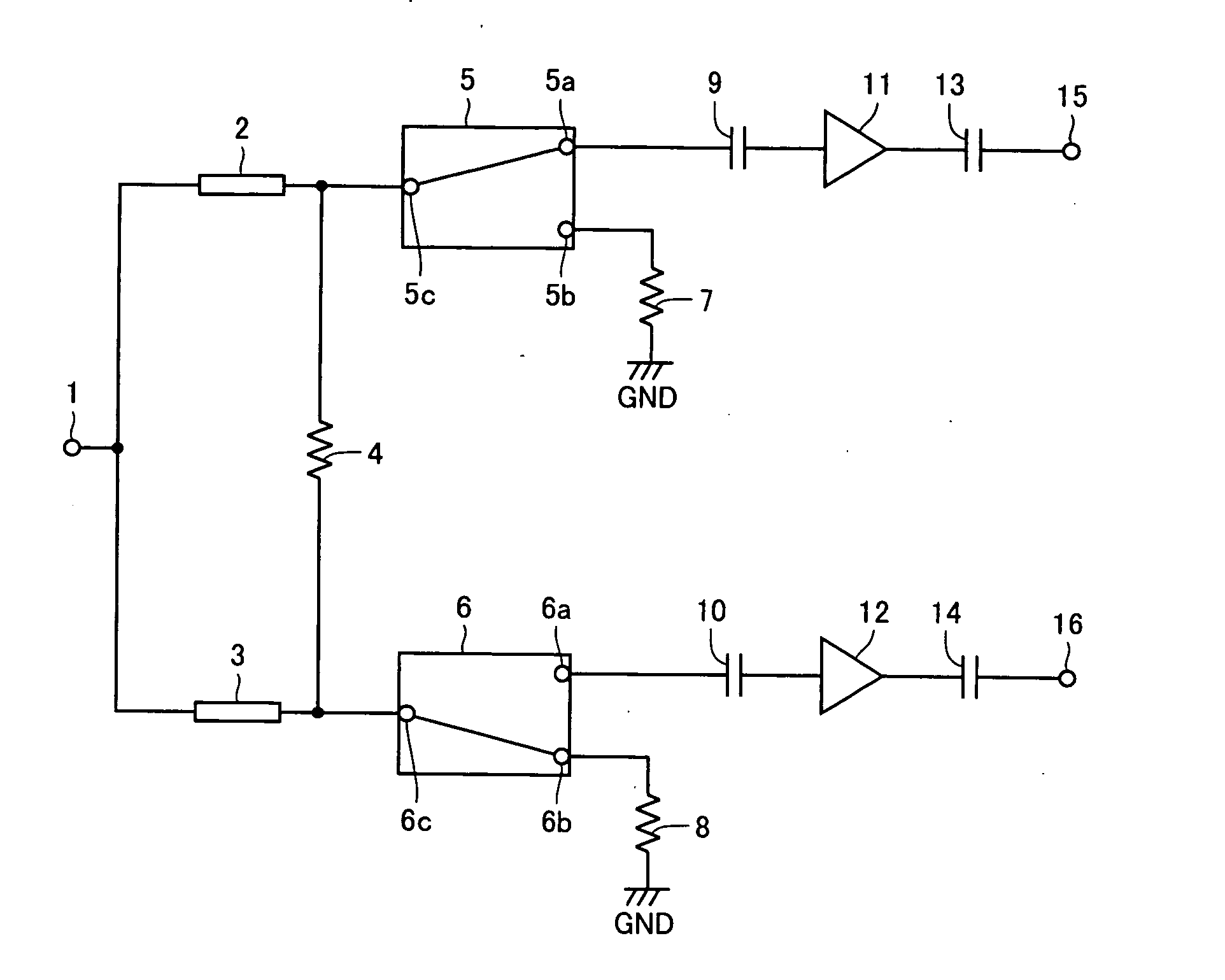
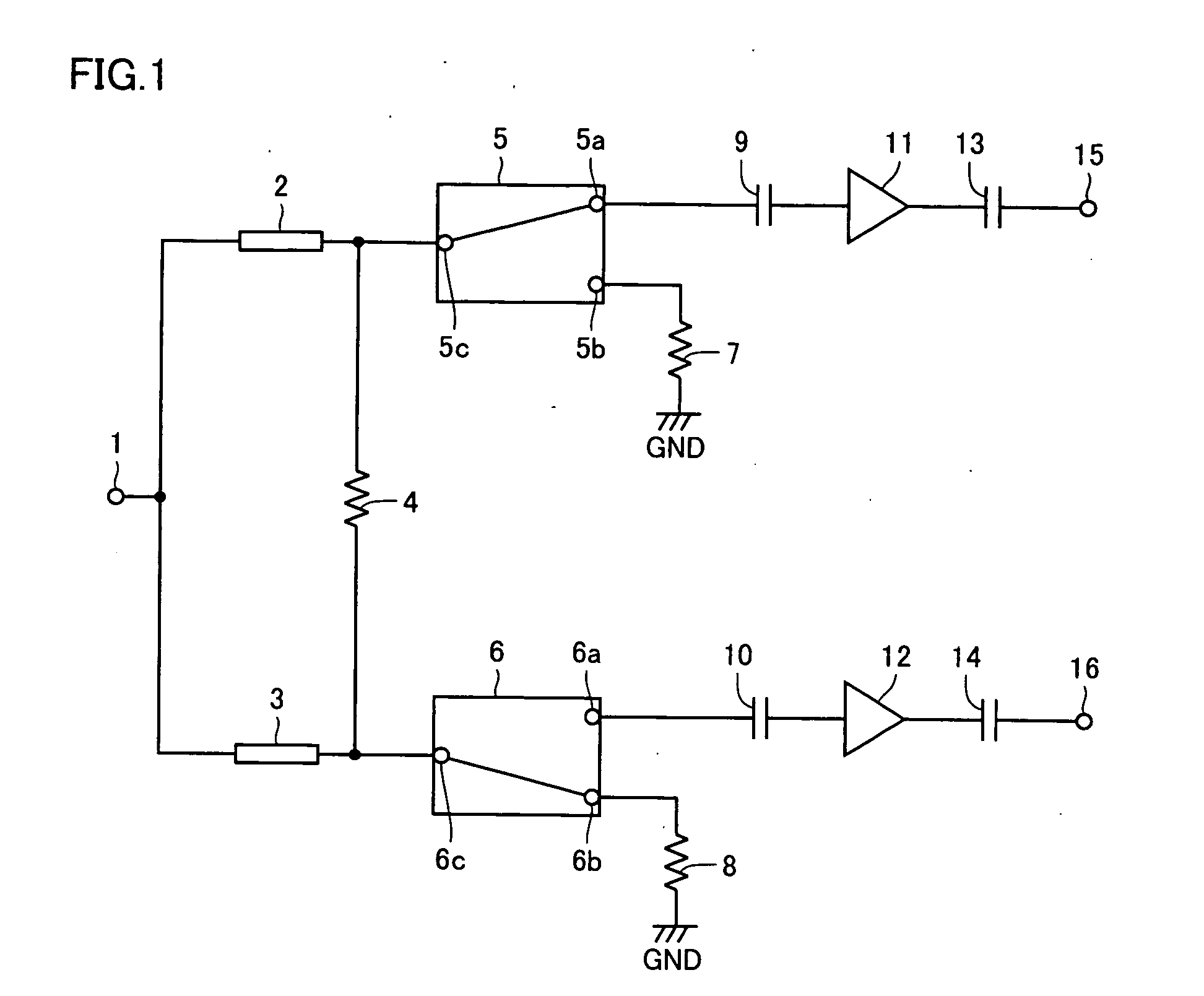
[0038]FIG. 1 is a circuit diagram showing a configuration of the present high-frequency distribution circuit in a In FIG. 1 the high-frequency distribution circuit is provided in a LNB, a SW-BOX or the like and includes an input terminal 1, high-frequency lines 2 and 3, a resistor 4, switch circuits 5 and 6, terminator resistors 7 and 8, capacitors 9, 10, 13 and 14, amplifiers 11 and 12, and output terminals 15 and 16.

[0039] High-frequency lines 2 and 3 each have one end connected to input terminal 1, and have their respective other ends connected to switch circuits 5 and 6 at common terminals 5c and 6c, respectively. Resistor 4 has a sufficiently larger value in resistance than terminator resistors 7 and 8 and is connected between the other ends of high-frequency lines 2 and 3, respectively. High-frequency lines 2 and 3 is equal in dimension and characteristic impedance (e.g., 75 Ω).

[0040] Switch circuit 5 has a first conduction terminal 5a connected via capacitor 9 to an input n...

second embodiment

[0050] Second Embodiment

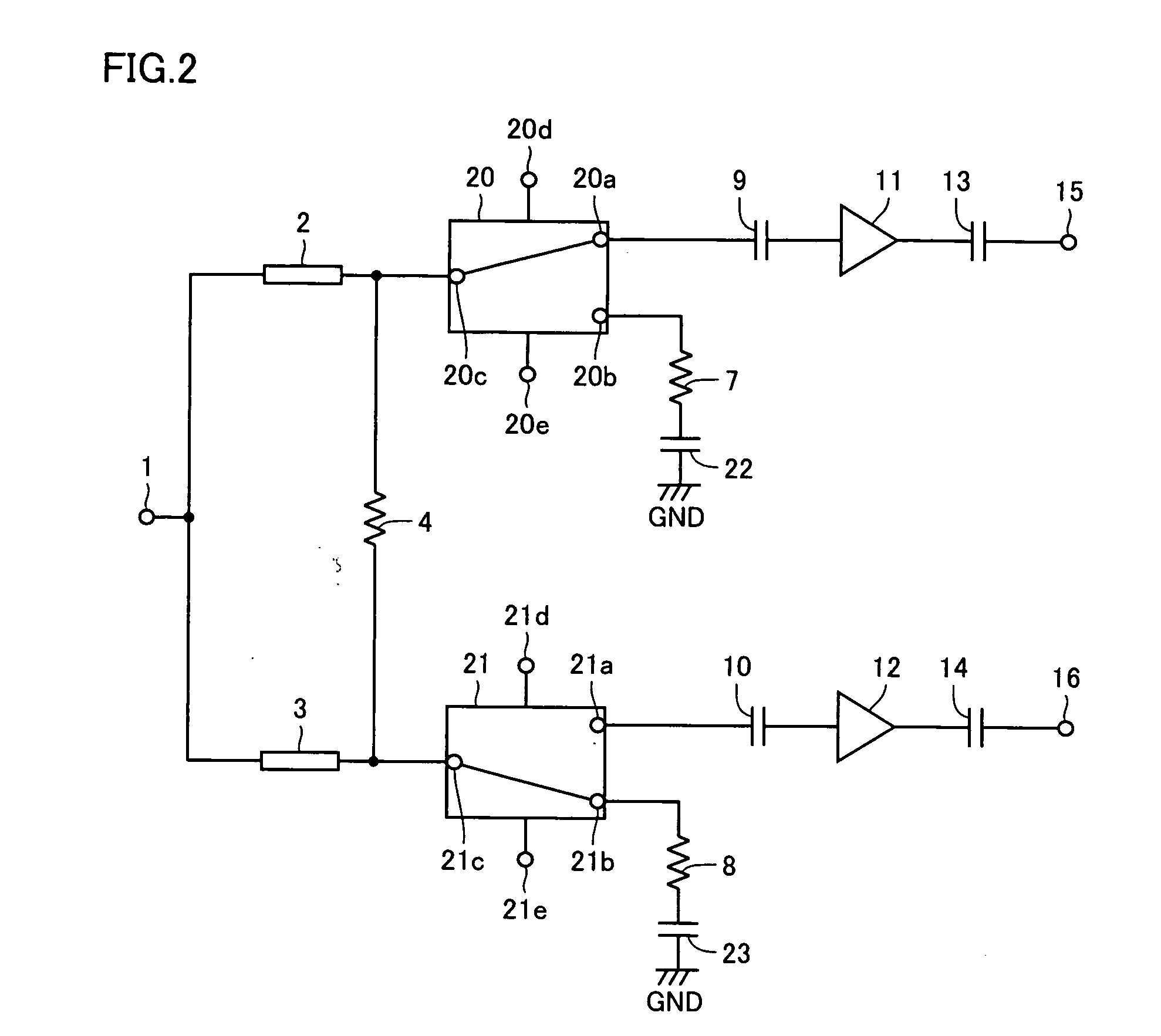
[0051]FIG. 2 is a circuit diagram showing a configuration of the present high-frequency distribution circuit in a second embodiment. The high-frequency distribution circuit of FIG. 2 corresponds to that of FIG. 1 with switch circuits 5 and 6 of FIG. 1 implemented by single pole double throws (SPDTs) 20 and 21, respectively.

[0052] SPDT 20 includes a common terminal 20c, first and second conduction terminals 20a and 20b, and first and second control terminals 20d and 20e. Common terminal 20c is connected to the other end of high-frequency line 2. The first conduction terminal 20a is connected via capacitor 9 to an input node of amplifier 11. The second conduction terminal 20b is connected via terminator resistor 7 and a capacitor 22 to a ground potential GND line. Capacitor 22 is provided to prevent a direct current (dc) current from flowing from the second conduction terminal 20b to the ground potential GND line and has a sufficiently low impedance for a high...

third embodiment

[0059] Third Embodiment

[0060]FIG. 3 is a circuit diagram showing a configuration of the present high-frequency distribution circuit in a third embodiment. The high-frequency distribution circuit of FIG. 2 corresponds to that of FIG. 1 with switch circuit 5 of FIG. 1 configured of PIN diodes 31 and 32, capacitors 33 and 34, a resistor 35 and first and second control terminals 36 and 37, and switch circuit 6 configured of PIN diodes 41 and 42, capacitors 43 and 44, a resistor 45 and first and second control terminals 46 and 47.

[0061] Capacitor 33 is connected between the other end of high-frequency line 2 and capacitor 9. Diode 31 has an anode connected to one terminal of terminator resistor 7 and has a cathode connected to a node located between capacitors 9 and 33. Diode 31 has resistance set to have a sufficiently small value when it conducts. Terminator resistor 7 has the other terminal connected via the first control terminal 36 and capacitor 34 to a ground potential GND line. C...


PUM


Abstract

The present high-frequency distribution circuit includes a switch circuit which passes a high-frequency signal from the other terminal of a high-frequency line to an output terminal if a receiver is connected to the output terminal and which grounds the other terminal of the high-frequency line via a terminator resistor if the receiver is not connected to the output terminal. As seen at an input terminal toward the output terminal, a constant value in resistance is provided regardless of whether the output terminal is used or not.

Description

[0001] This nonprovisional application is based on Japanese Patent Applications Nos. 2004-263990, 2005-039408, 2005-138352, and 2005-180657 filed with the Japan Patent Office on Sep. 10, 2004, Feb. 16, 2005, May 11, 2005, and Jun. 21, 2005, respectively, the entire contents of which are hereby incorporated by reference.BACKGROUND OF THE INVENTION [0002] 1. Field of the Invention [0003] The present invention relates generally to high-frequency distribution circuits and particularly to high-frequency distribution circuits distributing to a plurality of output terminals a frequency signal received at an input terminal. [0004] 2. Description of the Background Art [0005]FIG. 19 is a block diagram showing a configuration of a receiving unit of a satellite broadcast system as conventional. In FIG. 19 the satellite broadcast system has the receiving unit including an antenna 103 having a reflector 101 and a low noise block down converter (LNB) 102, receivers (or load circuits) 104 and 105, ...

Claims


Application Information

Patent Timeline
Patent Type & Authority Applications(United States)
IPC IPC(8): H04H1/00H04B1/18
CPCH04H40/90
Inventor KATO, MASAHIROHIRANO, TAKAOTANAKA, HITOSHI
Owner SHARP KK
Learn More