Metal polishing solution and polishing method

a metal polishing solution and metal technology, applied in the direction of detergent compounding agents, halogen oxide/oxyacids, other chemical processes, etc., can solve the problems of excessive polishing of the entire surface to be polished, excessive polishing of the wiring, and scratching of the polishing surface, etc., to achieve good dishing performance and high polishing rate

Inactive Publication Date: 2006-09-28
FUJIFILM HLDG CORP +1
View PDF17 Cites 21 Cited by
  • Summary
  • Abstract
  • Description
  • Claims
  • Application Information

AI Technical Summary

Benefits of technology

[0034] (11) A chemical-mechanical polishing method comprising bringing the metal polishing solution described in any one of (1) to (10) above into contact with a surface to be polished, and creating a relative motion between the surface to be polished and the polishing solution and / or a polishing pad, thereby effecting the polishing.
[0035] According to the present invention, a polishing solution capable of satisfying both a high polishing rate and a good dishing performance is provided.

Problems solved by technology

However, when CMP is performed by using a metal polishing solution containing such a solid abrasive grain, there may arise, for example, a polishing scratch (scratching), a phenomenon that the entire surface to be polished is excessively polished (thinning), a phenomenon that the polished metal surface is recessed like a dish (dishing), or a phenomenon that the insulating material between metal wirings is excessively polished and moreover, the wiring metal surface is recessed like a dish (erosion).
Also, this technique has a problem in view of the cost, for example, the washing step which is usually performed after the polishing for removing the polishing solution remaining on the semiconductor surface becomes complicated due to use of a polishing solution containing a solid abrasive grain and furthermore, the solid abrasive grain needs to be precipitated and separated at the treatment of solution (waste solution) after the washing.
Particularly, chemical-mechanical polishing (CMP) is performed in the semiconductor production process for achieving higher integration or multilayer fabrication of a semiconductor device or the like, but there is a problem that due to load produced in the polishing step, a defect is generated in the interlayer insulating film with a low dielectric constant.
However, the chemical polishing method only by the dissolution activity has a problem in view of flatness due to generation of dishing or the like, as compared with CMP of selectively effecting chemical-mechanical polishing of a metal film in the convex part.
The dishing is excessive excavation of the wiring part and this means that the concave part is polished.
A slurry giving a high polishing rate for the convex part generally has a high polishing rate also for the concave part and it is very difficult to establish both a high polishing rate and a good dishing performance.
To solve this problem, for example, JP-A-2001-152135 discloses a method of compounding an organic particle and an inorganic particle to increase the pressure dependency of the polishing force, but the effect is not sufficient.

Method used


Image

  • Metal polishing solution and polishing method
  • Metal polishing solution and polishing method
  • Metal polishing solution and polishing method

Examples


example 1

[0214] A polishing solution shown below was prepared, subjected to a polishing test and evaluated.

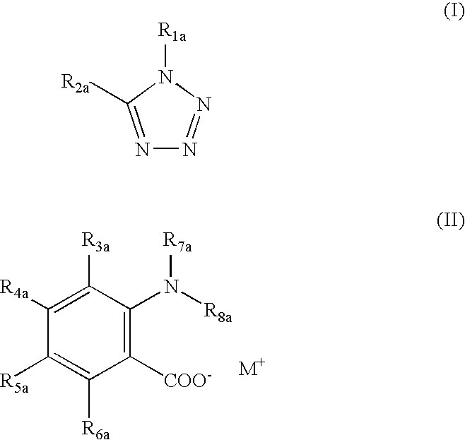
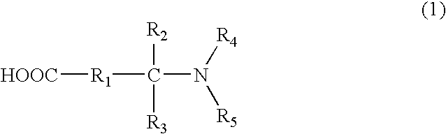
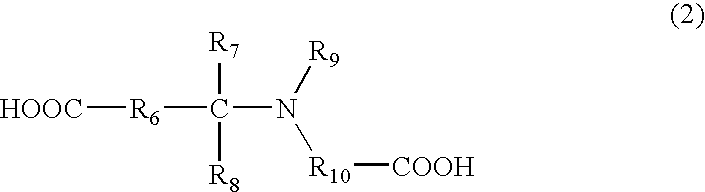
(Preparation of Polishing Solution)Colloidal silica (average particle diameter: 30 nm)Heteroaromatic ring compound or benzotriazole (BTA)0.001MHydrogen peroxide (oxidizing agent)15g / LCompound represented by formula (1) or (2) of glycine0.08MDodecylbenzenesulfonic acid (DBS) (in an amountshown in Table 3)Pure water added to make a total amount of1,000mLpH adjusted to6.8

(Polishing Test)

[0215] Substrate: silicon substrate having formed thereon a copper / silver alloy film having a thickness of 1 μm

[0216] Polishing pad: IC1400K-Groove (produced by Rodel Corp.)

[0217] Polishing apparatus: LGP-612 (produced by LapmaSter FT Co.)

[0218] Pressing pressure: 240 g / cm2

[0219] Polishing solution supply rate: 170 mL / min

[0220] Wafer diameter: 200 mm

[0221] Wafer: Cu blanket wafer or pattern wafer CMP854 produced by Sematech Inc. (200 mm)

[0222] Rotation number of polishing pad / wafer: 95 / 95 rpm

(E...


PUM

PropertyMeasurementUnit
oxidation reaction rateaaaaaaaaaa
diameteraaaaaaaaaa
dielectric constantaaaaaaaaaa

Abstract

A metal polishing solution comprising an oxidizing agent, wherein assuming that an oxidation reaction rate immediately after an oxidation of a metal to be polished starts at its surface is E1 and an oxidation reaction rate when an oxidation reaction reaches a stationary state is E2, E1/E2 is 1.5 or more and a time required for reaching an oxidation reaction rate of (E1+E2)/2 is from 1 to 50 seconds.

Description

FIELD OF THE INVENTION [0001] The present invention relates to the production of a semiconductor device, more specifically, the present invention relates to a metal polishing solution for use in the wiring step of a semiconductor device, and also relates to a polishing method using the same. BACKGROUND OF THE INVENTION [0002] In the development of a semiconductor device as represented by a semiconductor integrated circuit (hereinafter referred to as “LSI”), high-density and high-integration fabrication by the fine multilayer wiring is recently demanded for obtaining a highly integrated high-speed semiconductor device. For realizing this, a technique of chemical-mechanical polishing (hereinafter referred to as “CMP”) is being used. This is a method used for polishing an insulating thin film (e.g., SiO2) or a metal thin film used for wiring, thereby smoothening the substrate or removing an excess metal thin film produced at the wiring formation, and is disclosed, for example, in U.S. ...

Claims


Application Information

Patent Timeline
Patent Type & Authority Applications(United States)
IPC IPC(8): C11D3/39
CPCC09G1/02H01L21/3212C09K3/14
Inventor YAMASHITA, KATSUHIRO
Owner FUJIFILM HLDG CORP
Why Eureka
Try Eureka