Intrument for testing solid-state imaging device

a solid-state imaging and testing apparatus technology, applied in the direction of individual semiconductor device testing, television systems, instruments, etc., can solve the problems of difficult to improve the testing efficiency, difficult to align the handler, and restricted degree of freedom, and achieves convenient alignment and high-efficiency testing. , the effect of high efficiency

Inactive Publication Date: 2006-09-28
INTER ACTION
View PDF4 Cites 27 Cited by
  • Summary
  • Abstract
  • Description
  • Claims
  • Application Information

AI Technical Summary

Benefits of technology

[0009] An object of the present invention is to provide a testing apparatus, and a relay device and an optical module used in the testing apparatus; by which an optical system for irradiating a test light to a solid-state imaging device is easi

Problems solved by technology

However, since there are a probe card and a socket board between the optical system and the solid-state imaging device, the degree of freedom is restricted by their existence in a positional relationship of the optical system and the solid-state imaging device.
Therefore, it is difficult to improve the testing efficiency.
Also, the solid-state imaging device is mounted on the testing

Method used


Image

  • Intrument for testing solid-state imaging device
  • Intrument for testing solid-state imaging device
  • Intrument for testing solid-state imaging device

Examples


first embodiment

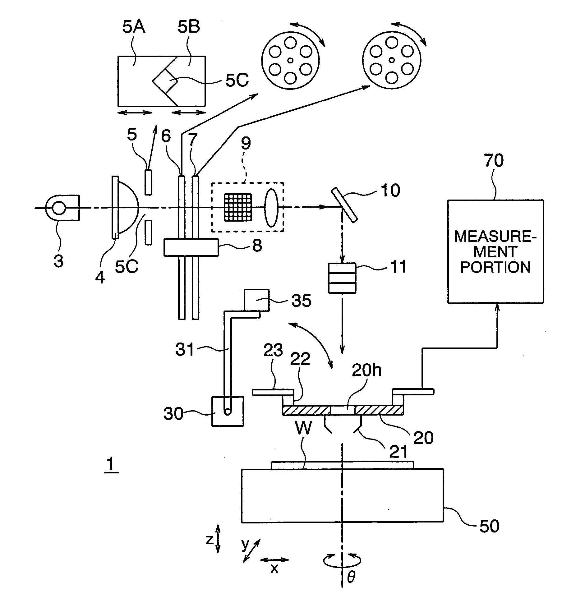
[0031]FIG. 1 is a view of the configuration of a testing apparatus of a solid-state imaging device according to an embodiment of the present invention.

[0032] In FIG. 1, a testing apparatus 1 has a light irradiation portion 2, a wafer table 50 and a measurement portion 70.

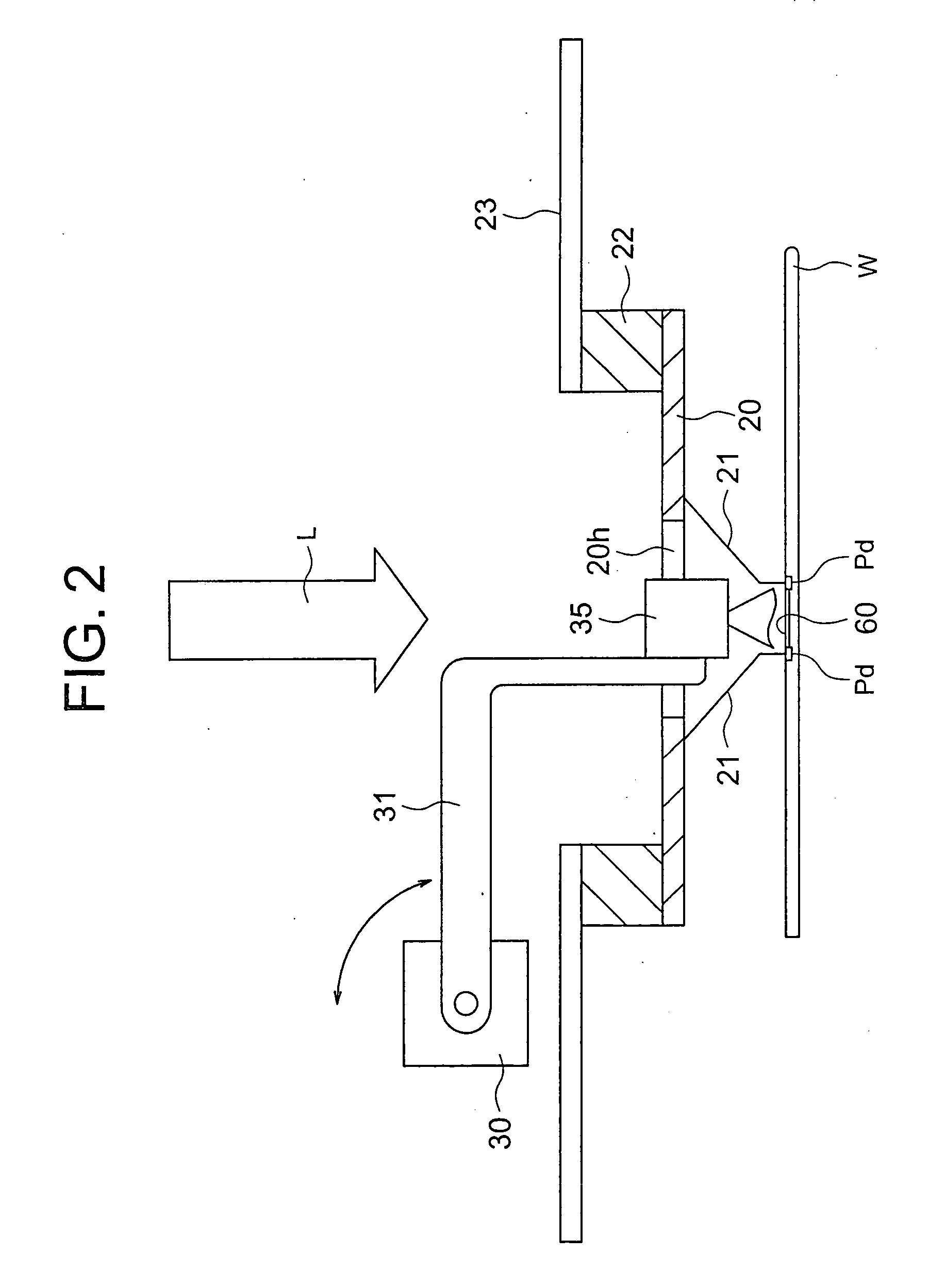
[0033] The light irradiation portion 2 has a light source 3, a condensing lens 4, a mechanical slit 5, an ND filter turret 6, a color filter turret 7, a homogenizer 9, a reflection mirror 10, a homogenizer 11, an optical module 35, a motor 30 and a holding arm 31.

[0034] The optical module 35 is an embodiment of the optical module of the present invention, and the motor 30 and the holding arm 31 compose an embodiment of the module moving means of the present invention.

[0035] As the light source 3, for example, a halogen lamp, a xenon lamp, and a metal halide lamp, etc. is used. The light source 3 reflects and condenses an emitted light to be in a predetermined direction.

[0036] The condensing lens 4 concentrates ...

second embodiment

[0071]FIG. 4 is a view showing the configuration of a probe card as a relay device according to another embodiment of the present invention. Note that the same reference numbers are used for the same components as those in the first embodiment in FIG. 4.

[0072] In FIG. 4, in a probe card 20A according to the present embodiment, an optical module 35 having the same configuration as that in the first embodiment is fixed to an opening portion 20h.

[0073] The optical module 35 is fixed by a fixing member 70.

[0074] A position of the optical module 35 with respect to a light receiving surface 60 is suitably adjusted in accordance with a solid-state imaging device to be tested.

[0075] The probe card 20A is held by a mother board 23 via the above pogo tower 22.

[0076] According to the present embodiment, it is not necessary to move the optical module 35 as in the first embodiment to test photoelectric conversion characteristics of the solid-state imaging device formed on the wafer W. There...

third embodiment

[0077]FIG. 5 is a view showing the configuration of a probe card as a relay device according to another embodiment of the present invention, and FIG. 6 is a sectional view along the line A-A in FIG. 5.

[0078] A probe card 200 shown in FIG. 5 has a card body 201 and an optical module 300.

[0079] The card body 201 of the probe card 200 basically has the same function as that of the probe cards according to the above explained embodiments, but it is different in a point that a plurality of (four) solid-state imaging devices can be tested at a time.

[0080] The probe card 200 is held by a mother board 23 via the above pogo tower 22.

[0081] The optical module 300 is provided at the center portion of the card body 201 having a disk shape.

[0082] As shown in FIG. 6, the optical module 300 is provided with holding members 301, optical lenses 302, diffusion plates 303, pin holes 304, and cover members 305.

[0083] The holding member 301 is formed with a plurality of holes 301h for forming ligh...


PUM


Abstract

A testing apparatus, by which an optical system to irradiate a test light to a solid-state imaging device is easily aligned with the solid-state imaging device and highly efficient tests can be conducted, is provided.
It includes an optical module 35 for irradiating a light from a light source to a light receiving surface of the solid-state imaging device through a pin hole, a probe card 20 having contact probes for contacting pads of the solid-state imaging device, and a motor 30 and a holding arm 31 for moving the optical module 35 to a predetermined position corresponding to the solid-state imaging device to be tested through an opening 20h provided to the probe card 20 in a state where the contact probes 21 contact the pads of the solid-state imaging device to be tested.

Description

TECHNICAL FIELD [0001] The present invention relates to a testing apparatus of a solid-state imaging device, and a relay device and an optical module used for testing a solid-state imaging device. BACKGOUND ART [0002] In a production process of a solid-state imaging device, such as a CCD (Charge Coupled Device) and a CMOS (Complementary Metal Oxide Semiconductor), testing of photoelectric conversion characteristics of the solid-state imaging device is necessary. In the testing, there are pre-process tests conducted in a chip state where the solid-state imaging device is formed on a semiconductor wafer and post-process tests conducted after the solid-state imaging device is assembled and packaged. [0003] In the pre-process tests, for example, in a state where a test head and a solid-state imaging device are electrically connected by using a probe card, a test light is irradiated to a light receiving surface of the solid-state imaging element through a predetermined optical system hav...

Claims


Application Information

Patent Timeline
IPC IPC(8): G01R31/308
CPCH04N17/002
Inventor TAMAI, SHINGO
Owner INTER ACTION
Why Eureka
Try Eureka