This helps you quickly interpret patents by identifying the three key elements:
Problems solved by technology
Method used
Benefits of technology
Benefits of technology
[0016] The present invention intends to provide a mold for nano-imprinting having fine projections-and-depressions (hereinafter referred to as unevens), the mold being prepared by a simple process with high reproducibility, and being capable of coping with warp and bend caused by repeated use. The present invention intends also to provide a process for preparation of the above mold.
[0034] The mold for nano-imprinting of the present invention has a fine concavo-convex pattern and is capable of coping with warp and bend caused by repeated use. The mold for nano-imprinting can be prepared with high reproducibility through a simple and precise process.
Problems solved by technology
This makes the mold preparation process complicated.
Further, dissolution of the resist by the plating solution, and other problems should be taken into account.
Method used
Image
Click on the blue label to locate the original text in one second.
Reading with bidirectional positioning of images and text.
Examples
example 1
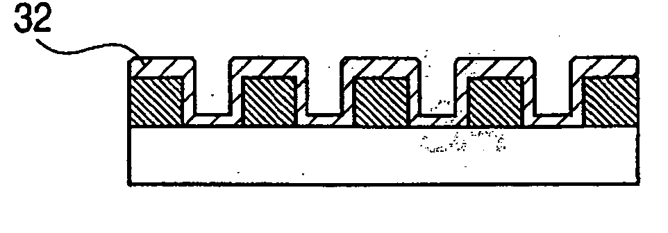
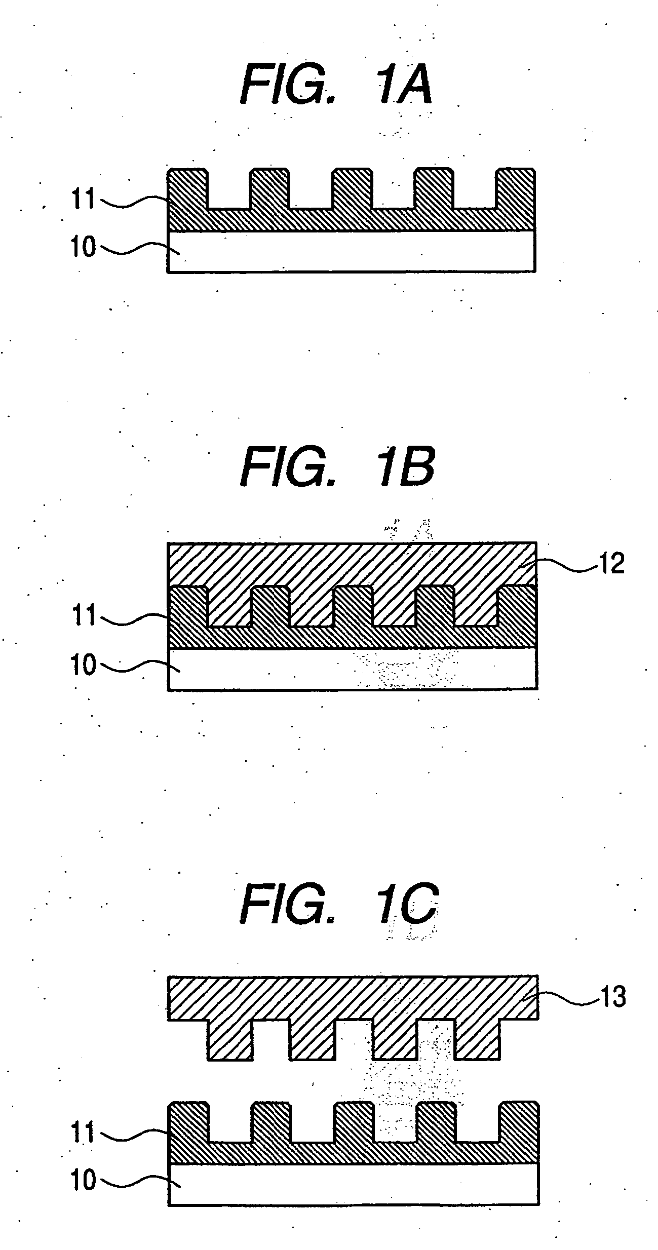
[0056] In this Example, a mold is prepared from a NiTi alloy by use of a resist pattern according to the present invention.
[0057] Firstly, by use of a mask formed by electron beam exposure, a 5-mm square mater mold was prepared which has projections of Si in a circular truncated cone shape of about 80 nm high arranged at intervals of 100 nm in a triangular lattice.
[0058] Next, on another Si substrate, an electron beam resist was applied in a thickness of about 50 nm by spin coating. With this resist-coated substrate kept heated at 120° C., the above master mold was pressed against the resist layer at a pressure of 1 ton / cm2.
[0059] After the substrate was cooled, the master mold was separated from the resist layer. The surface of the resist layer was examined by AFM (atomic force microscopy), and found that the projections of the master mold had been transferred as depressions onto the resist layer with the depression depth of about 40 nm and the depression diameter of about 60 nm...
example 2
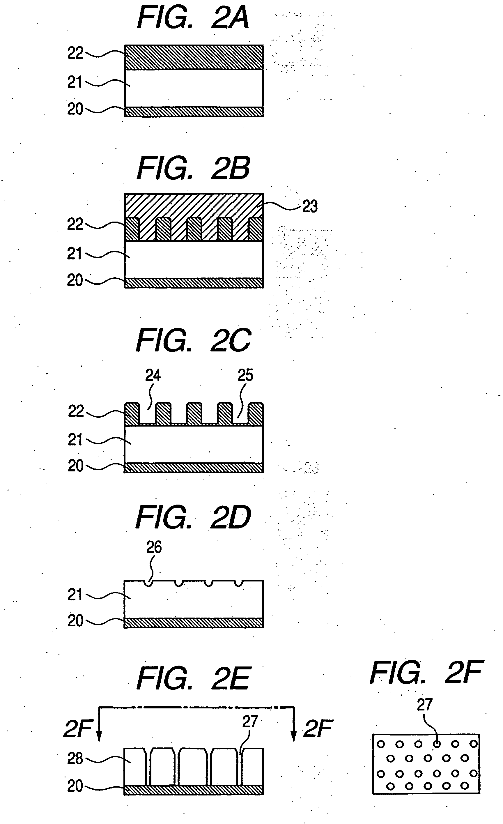
[0068] In this Example, nano-imprinting was conducted with the NiTi mold prepared in Example 1. In particular, with a nano-imprint employing the NiTi mold, aluminum was anodized to prepare highly regular porous film.
[0069]FIGS. 2A, 2B, 2C, 2D, 2E and 2F are drawings for explaining the nano-imprinting process employing the NiTi mold in this Example.
[0070] The nano-imprinting process with the NiTi mold in this Example is explained by reference to FIGS. 2A, 2B, 2C, 2D, 2E and 2F.
[0072] Secondly, with the substrate kept heated at 120° C., the NiTi mold 23 prepared in Example 1 was pressed against resist layer 22 at a pressure of 1 ton / cm2 (FIG. 2B).
[0073] After cooling the substrate, NiTi mold 23 was separated and removed (FIG. 2C).
[0074] The surface of separated resist layer 22 was...
PUM
Property
Measurement
Unit
Thickness
aaaaa
aaaaa
Ratio
aaaaa
aaaaa
Shape
aaaaa
aaaaa
Abstract
A novel mold is provided. The mold is prepared through steps of forming concavo-convex pattern on substrate, forming a film by embedding material of a composition having shape-memory in the concavo-convex pattern, and forming mold having the concavo-convex pattern by separating the film from the concavo-convex pattern after the film formation in the film formation step.
Description
BACKGROUND OF THE INVENTION [0001] 1. Field of the Invention [0002] The present invention relates to a mold, and a process for production of the mold. The present invention relates also to a member having a concavo-convex pattern prepared by use of the mold. [0003] 2. Related Background Art [0004] A typical technique for transferring a pattern on a substrate employed in semiconductor processes is a light exposure technique. In conventional light exposure techniques, integrated circuits of semiconductors have been made finer with remarkable improvement in the resolution by a fine processing technique for light exposure with a shorter wavelengthlight source and with progress of the optical system. At the moment, exposure of an extremely fine pattern of 100 nm or finer can be conducted by an ArF excimerlaser (λ=193 nm). For finer pattern, a F2 excimerlaser (λ=157 nm), EUV (extreme UV), X-rays, and-electron beams are investigated as the next-generation exposure techniques. [0005] How...
Claims
Application Information
Patent Timeline
Application Date:The date an application was filed.
Publication Date:The date a patent or application was officially published.
First Publication Date:The earliest publication date of a patent with the same application number.
Issue Date:Publication date of the patent grant document.
PCT Entry Date:The Entry date of PCT National Phase.
Estimated Expiry Date:The statutory expiry date of a patent right according to the Patent Law, and it is the longest term of protection that the patent right can achieve without the termination of the patent right due to other reasons(Term extension factor has been taken into account ).
Invalid Date:Actual expiry date is based on effective date or publication date of legal transaction data of invalid patent.

