
Nanolaminate thin films and method for forming the same using atomic layer deposition

Inactive Publication Date: 2006-09-28
VEECO INSTR +1
View PDF84 Cites 14 Cited by
  • Summary
  • Abstract
  • Description
  • Claims
  • Application Information

AI Technical Summary

Benefits of technology

[0006] In accordance with the present invention, the disadvantages and problems associated with fabricating a high quality nanolaminate thin film have been substantially reduced or eliminated. In a particular embodiment, a method is disclosed for forming a nanolaminate thin film of aluminum oxide and silicon dioxide on a substrate surface.
[0010] Important technical advantages of certain embodiments of the present invention include nanolaminate films formed using an ALD process that have high dielectric breakdown strengths. For certain applications, such as gap fill layers in read heads included in hard disk drives, the thickness of the film should be below a minimum value and the film should have certain characteristics. Single layer oxide films, such as aluminum oxide (Al2O3), may have lower breakdown fields at thickness below, for example, approximately 200 Å. A nanolaminate of Al2O3 and silicon dioxide (SiO2) having a thickness at or below approximately 200 Å, however, has a higher breakdown field due to the addition of SiO2 to the film and may be used to form high quality gap layers for read heads of high density hard disks.
[0012] A further important technical advantage of certain embodiments of the present invention includes nanolaminate films formed using an ALD process that have lower film stress. In many applications, it may be important for a thin film to have low stress. Single layer Al2O3 films formed using an ALD process may exhibit a high tensile stress, which is undesirable for applications such as gap layers of read heads in hard disk drives. SiO2 films formed using the ALD process, however, typically have a low tensile or compressive stress. Therefore, the film stress of an Al2O3 / SiO2 nanolaminate may be controllably reduced by adding SiO2 to decrease the Al2O3 concentration of the film.

Problems solved by technology

At thicknesses below 200 Å, however, Al2O3 films typically have a lower dielectric strength and are more susceptible to resist developer etch.
In addition, conventionally sputtered gap layers may not be suitable for higher recording densities because they are difficult to reliably scale below 300 Å due to excessive leakage currents.
Although ion beam deposited gap layers can be scaled down in thickness to below 300 Å, such layers tend not to be adequately conformal.

Method used


Image

  • Nanolaminate thin films and method for forming the same using atomic layer deposition
  • Nanolaminate thin films and method for forming the same using atomic layer deposition
  • Nanolaminate thin films and method for forming the same using atomic layer deposition

Examples


Embodiment Construction

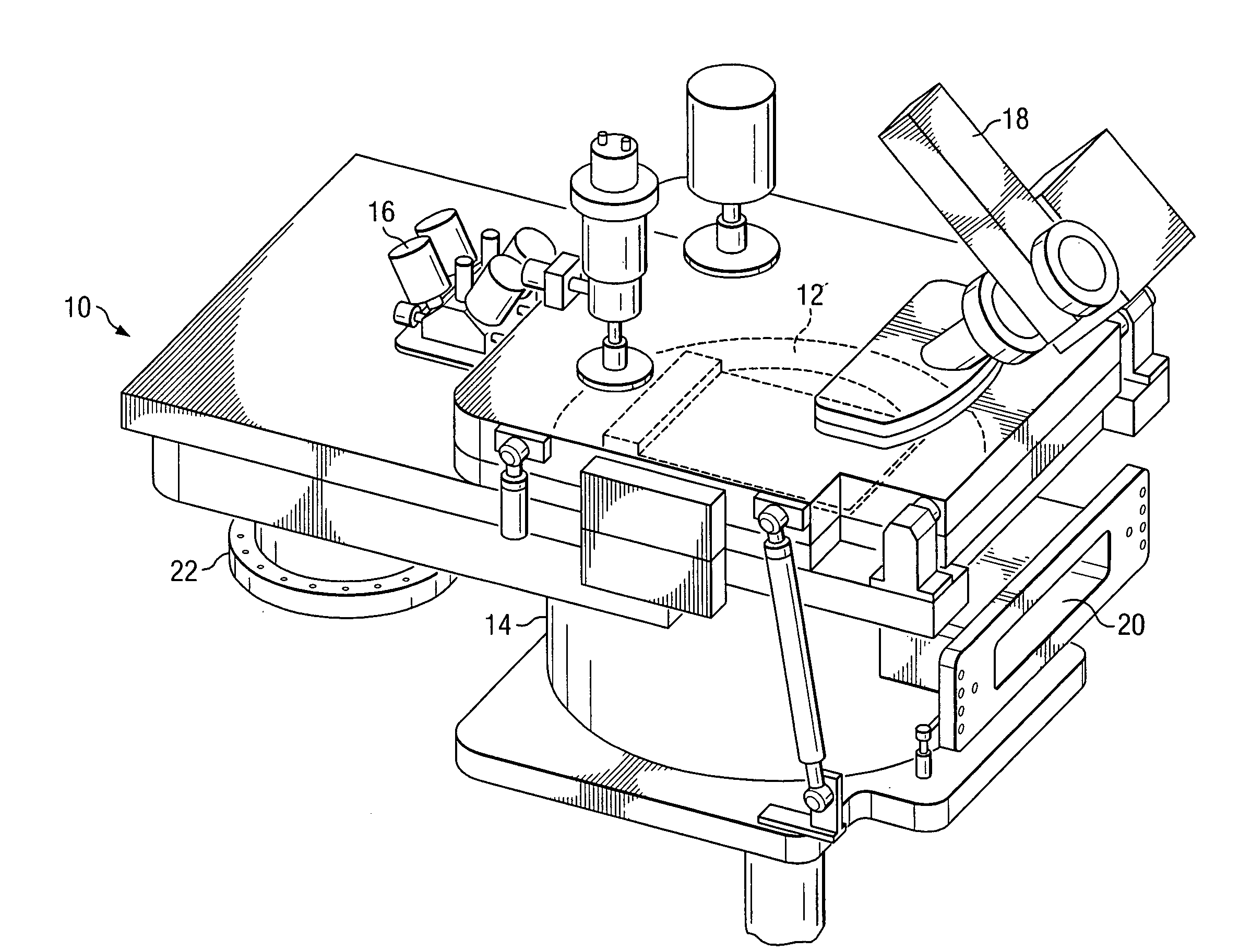
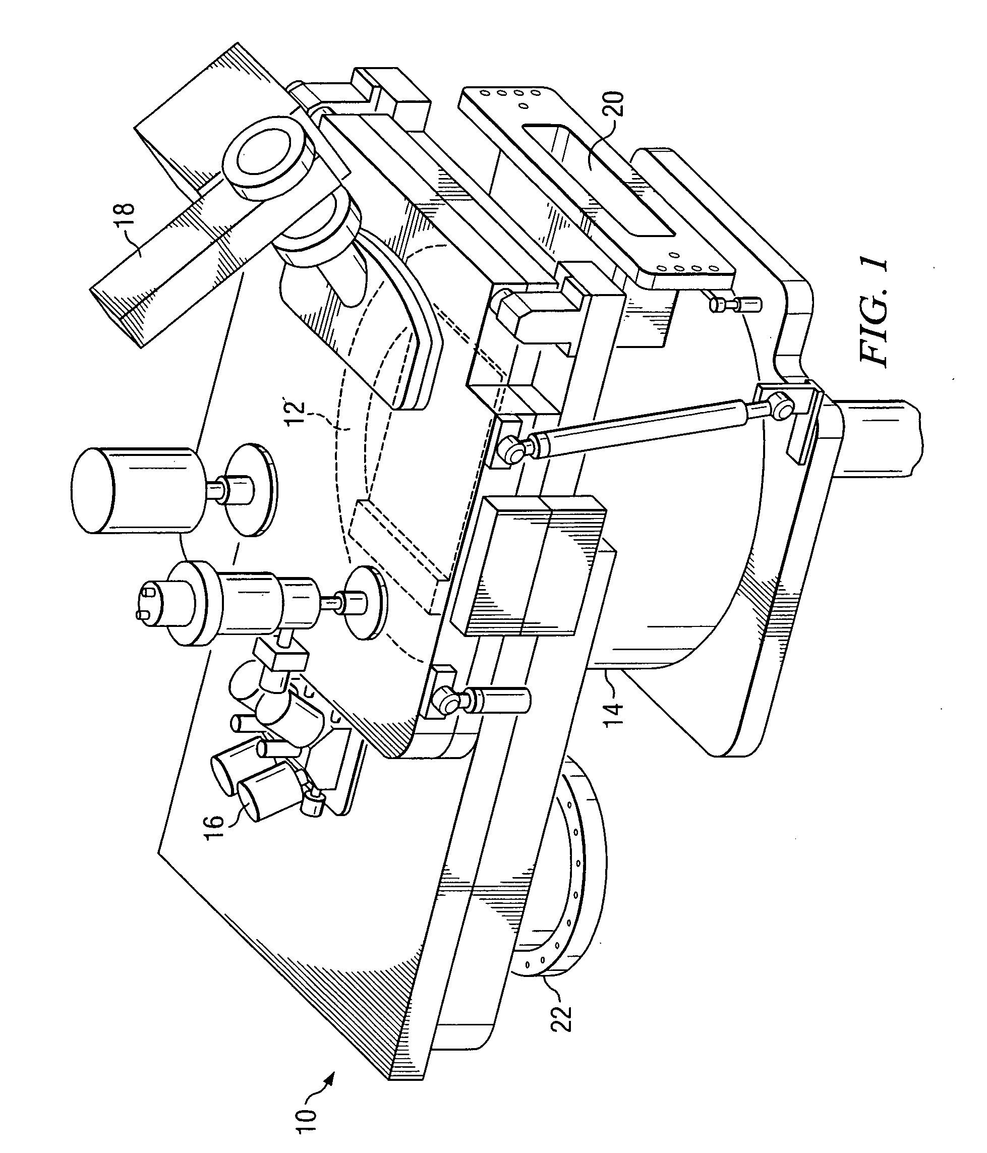
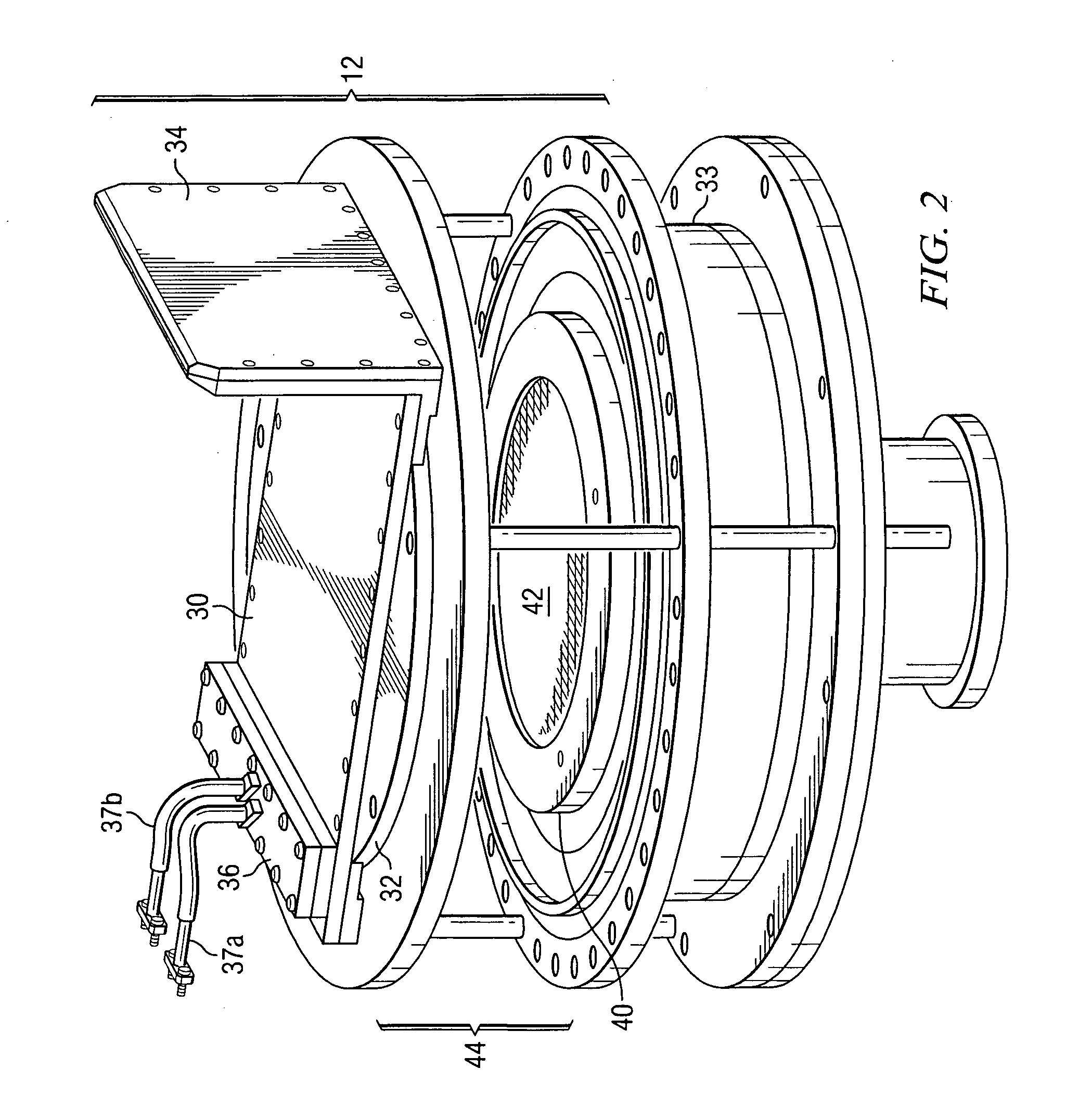
[0029] Preferred embodiments of the present invention and their advantages are best understood by reference to FIGS. 1 through 10, where like numbers are used to indicate like and corresponding parts.

[0030] The conceptual groundwork for the present invention involves an atomic layer deposition (ALD) process to create highly conformal thin films. In an ALD process, a precursor and a reactant, such as a reactant gas are sequentially pulsed onto the surface of a substrate contained in a reaction chamber, without mixing the precursor and reactant in the gas phase. Each of the precursor and the reactant reacts with the surface of the substrate to form an atomic layer in such a way that only one layer of a material forms at a time. The introduction of the precursor and / or the reactant into the reaction chamber may be referred to as a doping pulse. In between doping pulses, the reaction chamber may be purged by flowing an inert gas over the substrate. One film that may be formed using an ...


PUM

PropertyMeasurementUnit
Temperatureaaaaaaaaaa

Abstract

A nanolaminate thin film and a method for forming the same using atomic layer deposition are disclosed. The method includes forming an aluminum oxide layer having a first thickness on at least a portion of a substrate surface by sequentially pulsing a first precursor and a first reactant into an enclosure containing the substrate. A layer of silicon dioxide is formed on at least a portion of the aluminum oxide layer by sequentially pulsing a second precursor and a second reactant into the enclosure to form a nanolaminate thin film.

Description

TECHNICAL FIELD OF THE INVENTION [0001] The present invention generally relates to film deposition, and more particularly to a nanolaminate thin film and method for forming the same using atomic layer deposition. BACKGROUND OF THE INVENTION [0002] Atomic layer deposition (ALD), also known as sequential pulsed chemical vapor deposition (SP-CVD), atomic layer epitaxy (ALE) and pulsed nucleation layer (PNL) deposition, has gained acceptance as a technique for depositing thin and continuous layers of metals and Dielectrics with high conformality. In an ALD process, a substrate is alternately dosed with a precursor and one or more reactant gases so that reactions are limited to the surface of a substrate. Thus, gas phase reactions are avoided since the precursor and the reactant gases do not mix in the gas phase. Uniform adsorption of precursors on the wafer surface during the ALD process produces highly conformal layers at both microscopic feature length scales and macroscopic substrate...

Claims


Application Information

Patent Timeline
IPC IPC(8): C23C16/00B32B9/00
CPCC23C16/402C23C16/45529C23C26/00C23C28/00C23C28/04H01L21/3142H01L21/31608H01L21/31616H01L21/02164H01L21/02178H01L21/022H01L21/0228
Inventor MAO, MINGBUBBER, RANDHIRSCHNEIDER, THOMAS ANDREW
Owner VEECO INSTR
Learn More