

Method for removing silicon oxide film and processing apparatus
- Summary
- Abstract
- Description
- Claims
- Application Information
AI Technical Summary
Benefits of technology
Problems solved by technology
Method used
Image

Examples
first embodiment
[0045] A silicon dioxide film removing method in a first embodiment according to the present invention and processing systems for carrying out the same will be described with reference to the accompanying drawings.
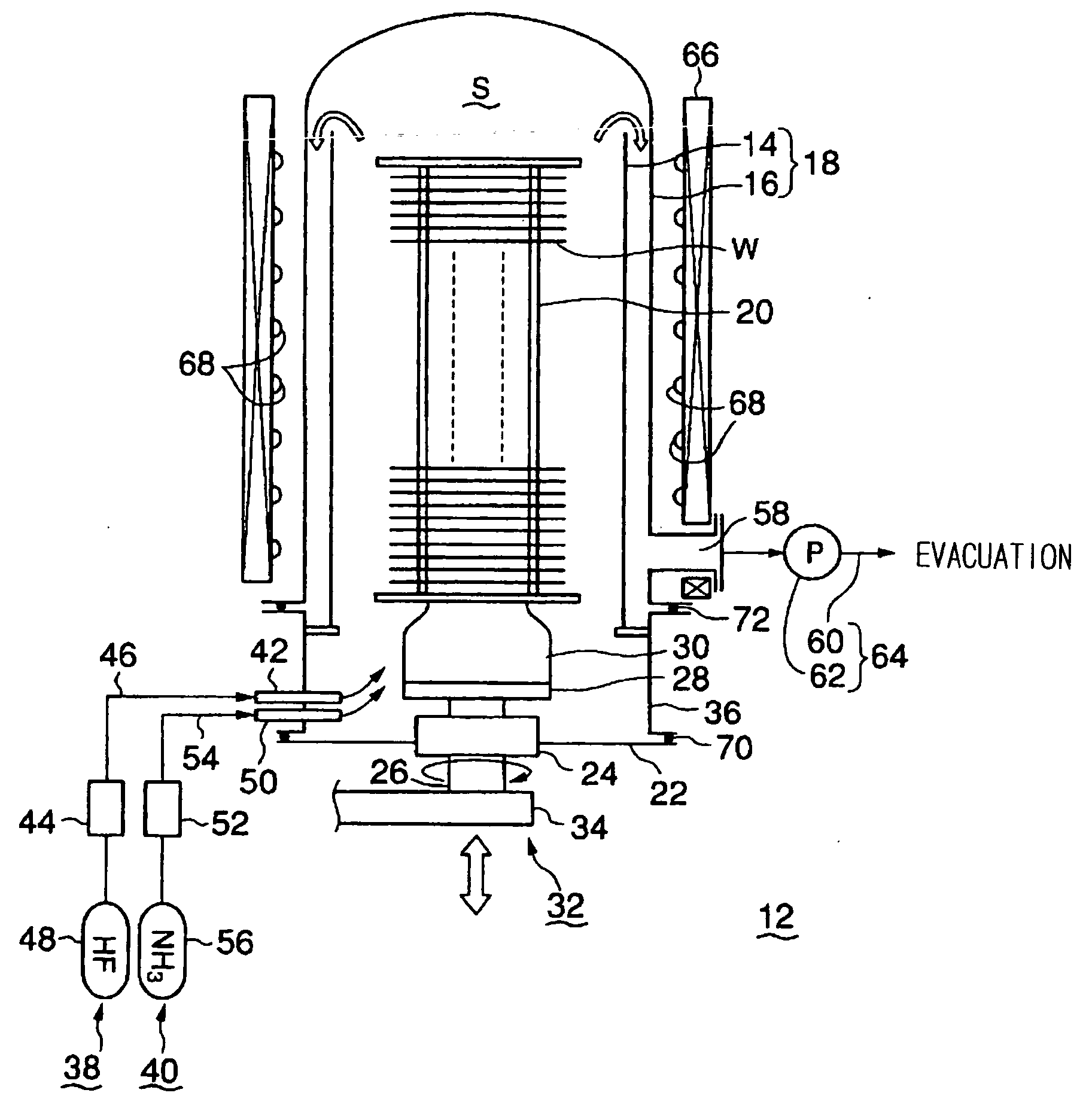
[0046]FIG. 1 shows a processing system 12 for carrying out a silicon dioxide film removing method in a preferred embodiment according to the present invention. The processing system 12 includes a double-wall, vertical processing vessel 18 of a predetermined length. The processing vessel 18 includes an inner tube 14 of quartz and an outer tube 16 of quartz. The inner tube 14 defines a processing space S. A wafer boat 20 of quartz, namely, a workpiece holding means, is placed in the processing space S. Semiconductor wafers W, namely, workpieces, are held in layers on the wafer boat 20 at predetermined vertical pitches. The pitches may be equal or may be different according to the positions of the wafers W.
[0047] A cap 22 closes and opens the lower end of the processing vess...
second embodiment
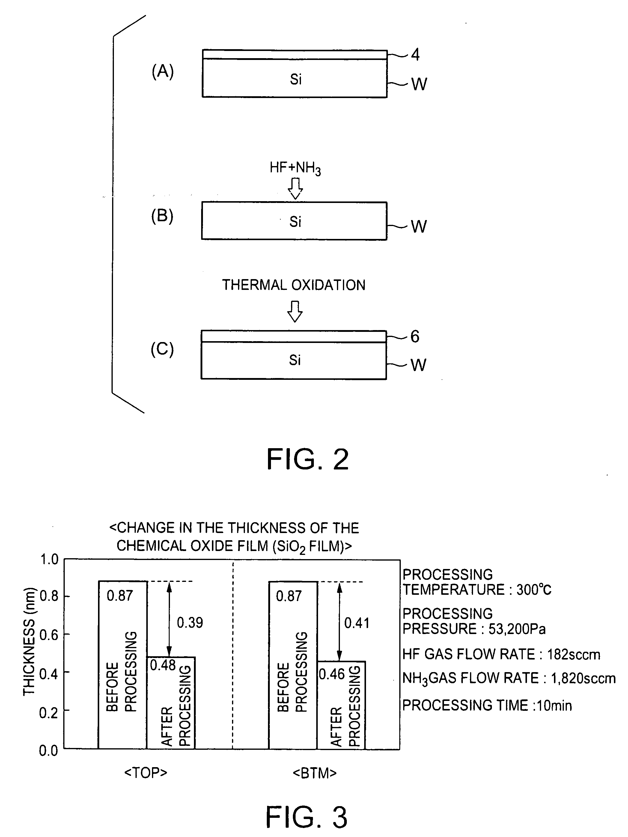
[0057] Then, a thermal oxide film 6 for forming, for example, a gate oxide film is formed on the wafer W as shown in FIG. 2(C) by another processing system. A silicon dioxide film removing method in a second embodiment, which will be described later, carries out both a film removing process for removing the chemical oxide film 4 and a film forming process for forming the thermal oxide film 6 by a single processing system.
[0058] A film removing method of removing the chemical oxide film 4 by the processing system 12 will be more specifically described.
[0059] As shown in FIG. 2(A), a plurality of semiconductor wafers W each having a surface coated with a chemical oxide film 4 are arranged in layers at predetermined pitches on the wafer boat 20. The boat elevator 32 raises the wafer boat 20 upward to load the wafer boat 20 through the lower end of the processing vessel 18 into the processing vessel 18. Then, the processing vessel 18 is sealed. The interior of the processing vessel 18 ...
PUM
| Property | Measurement | Unit |
|---|---|---|
| Temperature | aaaaa | aaaaa |
| Temperature | aaaaa | aaaaa |
| Temperature | aaaaa | aaaaa |
Abstract
Description
Claims
Application Information