

Vapor phase treatment of dielectric materials
a dielectric material and vapor phase technology, applied in the direction of coatings, chemical vapor deposition coatings, metallic material coating processes, etc., can solve the problems of power consumption and signal cross-talk becoming increasingly difficult to solve, reactive gases have been found to damage the carbon at the surface of dense materials, and new challenges have been identified during back end of line processing
- Summary
- Abstract
- Description
- Claims
- Application Information
AI Technical Summary
Benefits of technology
Problems solved by technology
Method used
Image

Examples
example 1
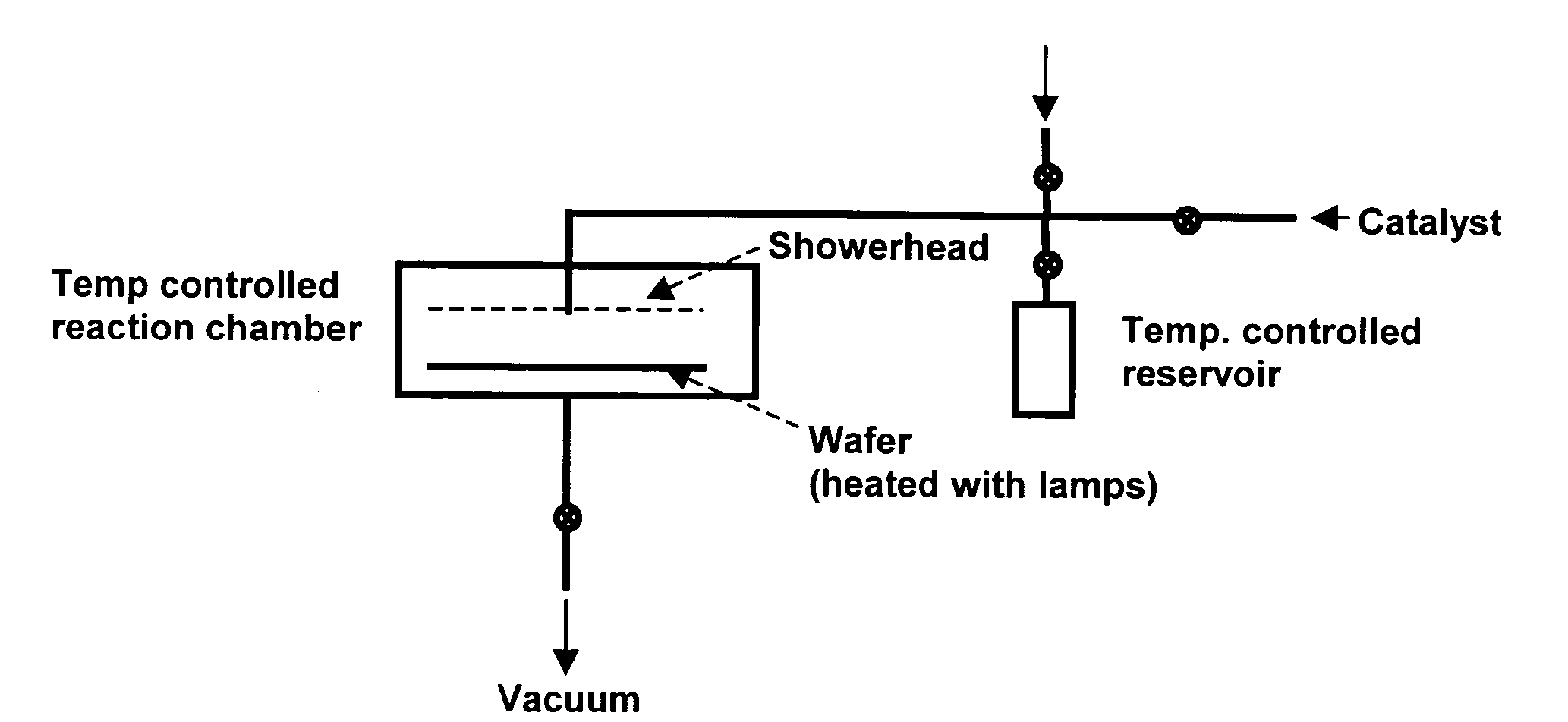
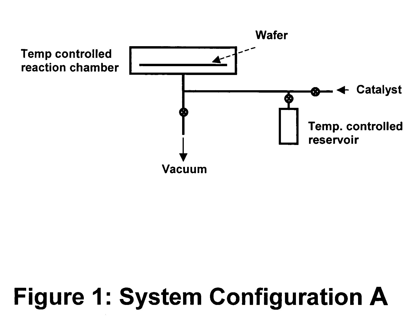
(System Configuration A)
[0103] The configuration shown in FIG. 1 was used to perform a silylation treatment. A reservoir was filled with 100% dimethyldiacetoxysilane (DMDAS). Reservoir temperature is adjustable. A wafer with plasma damaged porous low-k (NANOGLASS-E, commercially available form Honeywell International, Sunnyvale, California) was placed in the reaction chamber, evacuated for a 30 min dehydration step and during evacuation the film was heated to a desired temperature. The film was exposed to DMDAS vapor for desired time. The wafer was then removed from the reaction chamber and baked in N2 ambient on hot plates at 125° C., 200° C. and 350° C. for 1 minute each. The properties of the low-k film at different process steps are as follows. An increase in chamber process temperature increased %carbon repair and decreased dielectric constant. An increase in exposure time decreased carbon repair for lower temperature, but increased carbon repair for higher temperature proces...
example 2
(System Configuration A)
[0104] The configuration shown in FIG. 1 was used to perform a silylation treatment. A reservoir was filled with 100% DMDAS. The reservoir temperature is adjustable. A wafer with plasma damaged porous low-k (NANOGLASS-E) was placed in the reaction chamber, evacuated for a 30 min dehydration step and during evacuation the film was heated to a desired temperature. The film was exposed to DMDAS vapor for 1 min. Expose to NH3 for 1 minute. The wafer was then removed from the reaction chamber and baked in N2 ambient on hot plates at 125° C., 200° C. and 350° C. for 1 min each. The properties of the low-k film at different process steps are as follows. An increase in chamber process temp with 1 minute exposure decreased % carbon repair, but decreased dielectric constant. The condition with increased exposure time and higher chamber temp gave decreased % carbon repair and decreased dielectric constant.
Pumpdown PriorDMDASContact Angle% CarbonChamberDMDAS Exposure...
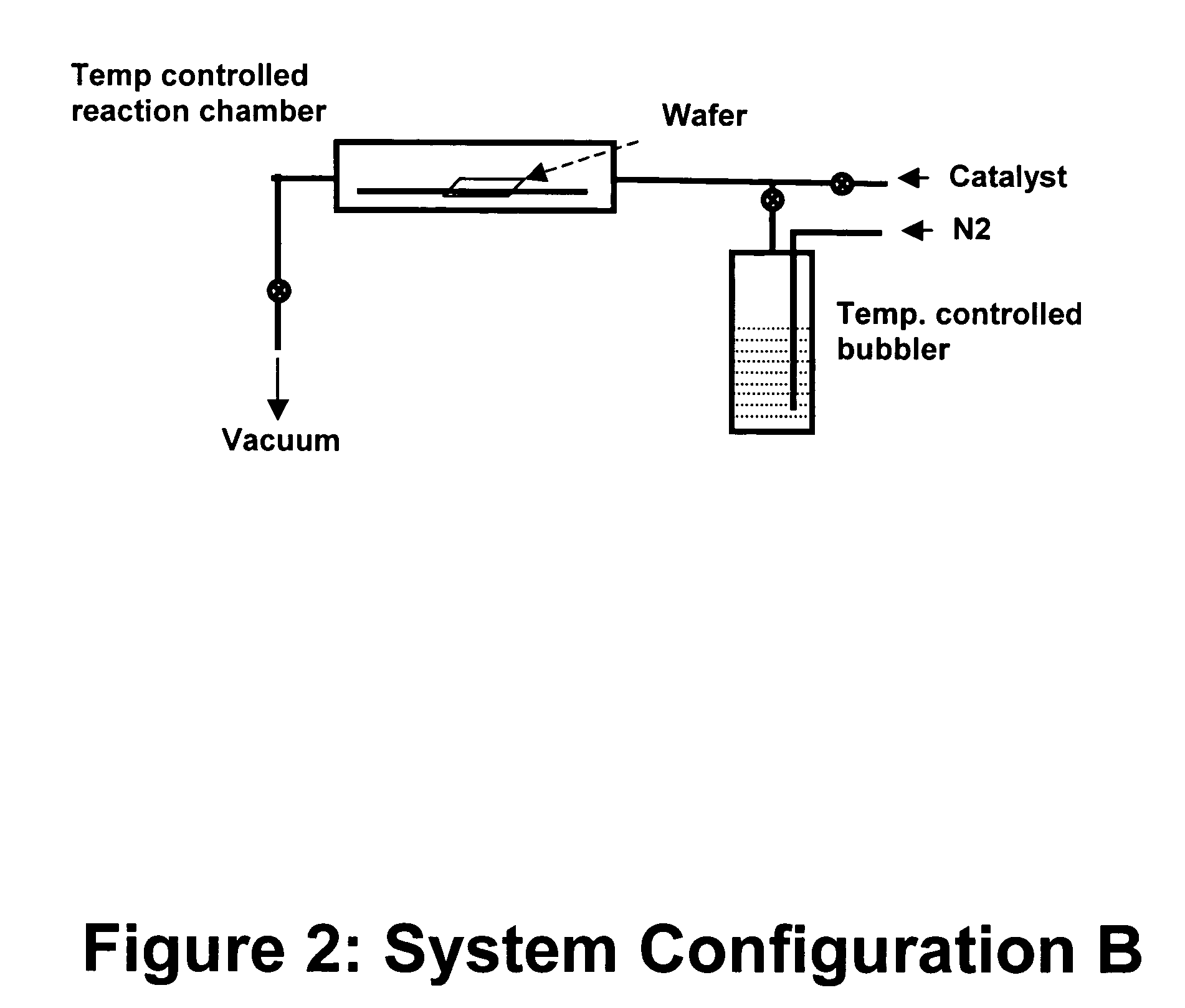
example 3
(System Configuration B)
[0105] The configuration shown in FIG. 2 was used to perform a silylation treatment. A bubbler was filled with 100% DMDAS and was maintained at a constant temperature of 45° C. Nitrogen was used to bubble through DMDAS and carry DMDAS through chamber at desired flow. A wafer with plasma damaged porous low-k (NANOGLASS-E) was placed in the furnace tube evacuated for 30min dehydration step while being heated to a desired temperature. The film was exposed to DMDAS vapor for 30 minutes. A final anneal was performed in the furnace tube at a desired temperature. The wafer was then removed from furnace tube. The properties of the low-k film at different process steps are as follows. Varied chamber temperature conditions gave similar contact angle. The % carbon repair varied throughout temperature range. A dielectric constant of 2.29 was result for one temperature condition.
Pumpdown PriorDMDASContact Angle% CarbonChamberFinalDMDAS ExposureExposure(NGE) PostRestor...
PUM
| Property | Measurement | Unit |
|---|---|---|
| Temperature | aaaaa | aaaaa |
| Temperature | aaaaa | aaaaa |
| Fraction | aaaaa | aaaaa |
Abstract
Description
Claims
Application Information