DC-DC converter
a converter and dc technology, applied in the direction of dynamo-electric converter control, process and machine control, instruments, etc., can solve the problems of low power conversion efficiency, unfavorable increase of manufacturing costs, and malfunction of devices connected to switching power sources, so as to reduce the power consumption of the oscillator, improve the switching efficiency, and reduce the loss of switching.
- Summary
- Abstract
- Description
- Claims
- Application Information
AI Technical Summary
Benefits of technology
Problems solved by technology
Method used
Image
Examples
first embodiment
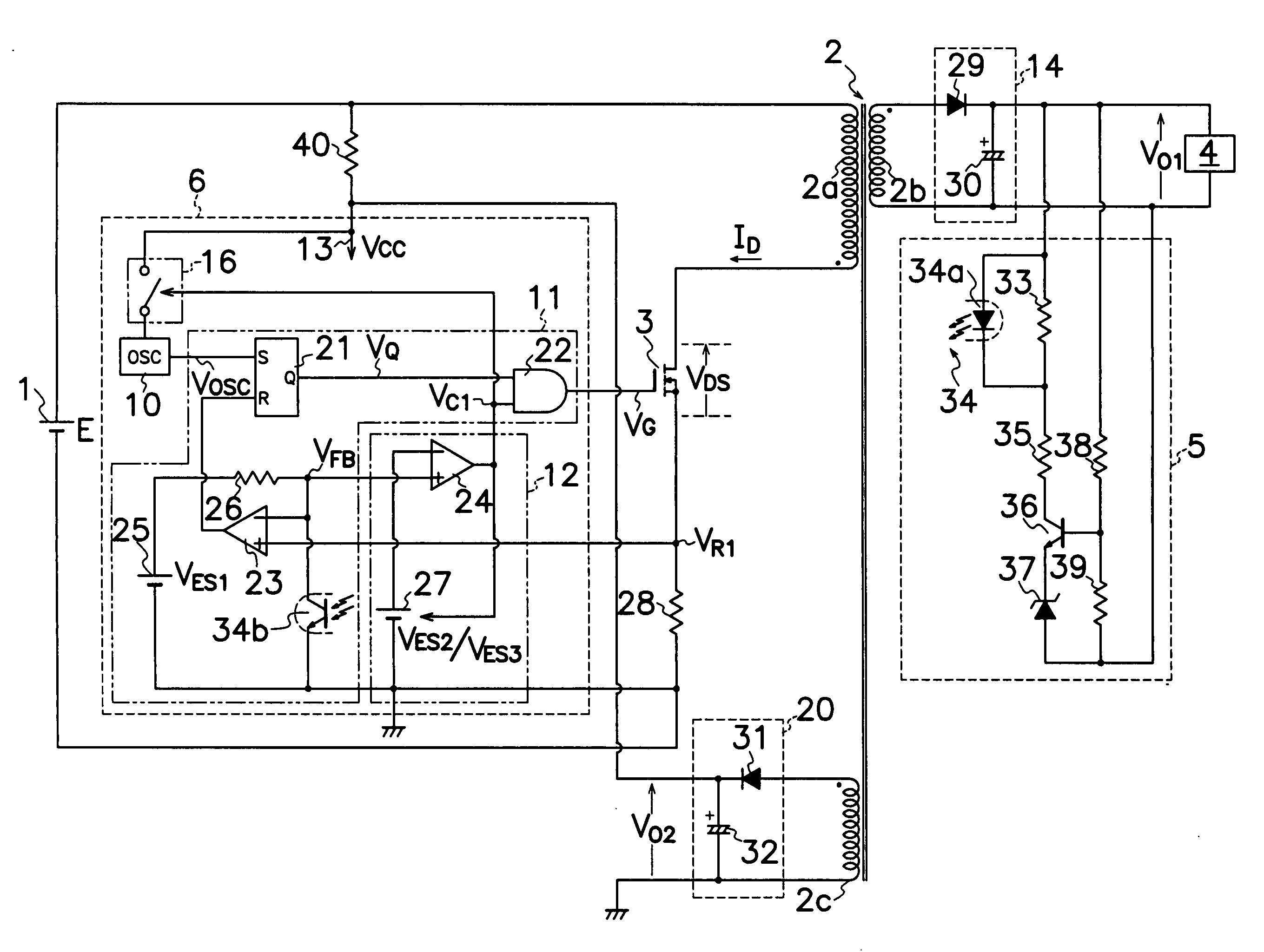
[0032]FIG. 7 shows power control circuit 16 which comprises a P-channel MOS-FET 17 as a switch element connected between a drive power source 13 and oscillator 10 to receive drive power VCC from drive power source 13. MOS-FET 17 is turned off when second comparator 24 of intermittent controller 12 produces the output of low voltage level VC1 to AND gate 22 of signal output circuit 11. Power control circuit 16 comprises a series circuit of resistors 45 and 46 and N-channel MOS-FET 47 connected in series between a junction of drive power source 13 and P-channel MOS-FET 17 and ground; a gate terminal of P-channel MOS-FET 17 is connected to a junction of resistors 45 and 46; and a gate terminal of N-channel MOS-FET 47 is connected to output terminal of second comparator 24 through a resistor 48.
[0033]FIG. 8 shows voltage waveforms in selected location of the circuit when MOS-FET 3 is converted to the intermittent operation during the light load period. When second comparator 24 produces...
second embodiment
[0034]FIG. 9 illustrates power control circuit 16, but otherwise, oscillator 10 comprises a signal generator 7 for producing pulse signals VOSC, and a power supplying circuit 8 for feeding drive power VCC to signal generator 7 of oscillator 10. Power supplying circuit 8 comprises a feed PNP transistors 9a to 9c as switches connected between drive power source 13 and signal generator 7 to receive drive power VCC from drive power source 13. Power control circuit 16 turns feed PNP transistors 9a to 9c off when second comparator 24 produces control signal VC1 of low voltage level to AND gate 22 of signal output circuit 11. Drive power VCC is modulated to a constant voltage through a voltage regulator 49 on which drive power VCC is applied, and supplied to oscillator 10. Power control circuit 16 comprises a series circuit of a first control PNP transistor 19, a resistor 50 and a second control NPN transistor 59 connected between voltage regulator 49 and ground, and a base terminal of sec...
PUM
 Abstract
Description
Claims
Application Information


