Semiconductor device and method of manufacturing the same

a technology of semiconductors and semiconductors, applied in the direction of semiconductor devices, basic electric elements, electrical appliances, etc., can solve the problems of further improvement of driving performance, disadvantage when mounted on a chip with other ic elements, and in the above-mentioned art, and achieve the effect of increasing the gate width per unit plan

Inactive Publication Date: 2006-10-05
ABLIC INC
View PDF2 Cites 21 Cited by
  • Summary
  • Abstract
  • Description
  • Claims
  • Application Information

AI Technical Summary

Benefits of technology

[0018] Further, according to the present invention, connection through thermal diffusion of the second conductivity type semiconductor region formed between the semiconductor substrate surface and the epitaxial film through the ion implantation with the second conductivity type semiconductor region formed through the oblique ion implantation after formation of the trench structure to the epitaxial. Thus, the well can be formed even deeper. Accordingly, the bottom surface of the concave portion can be formed even deeper, and consequently, the gate width per unit plane can be further increased.

Problems solved by technology

However, it is also a fact that lowering of withstanding voltage, which is caused by miniaturization of elements, hinders further improvement of the driving performance.
The transistor has extremely excellent performance as an element itself, but has a disadvantage when mounted on a chip with other IC elements.
The above-mentioned art has, however, two problems.
However, this method also has limitation on the length, and additionally has a risk such as the reduction in concentration of the source region 001 or the drain region 002 caused by the excessive impurity diffusion.
Actual implementation of the method is, therefore, difficult.
That is, it is difficult to increase the contact area in the conventional art without changing the element area to reduce the ON resistance of the MOS transistor.
(2) The second problem is that there is a limitation to the trench depth.

Method used


Image

  • Semiconductor device and method of manufacturing the same
  • Semiconductor device and method of manufacturing the same
  • Semiconductor device and method of manufacturing the same

Examples


embodiment

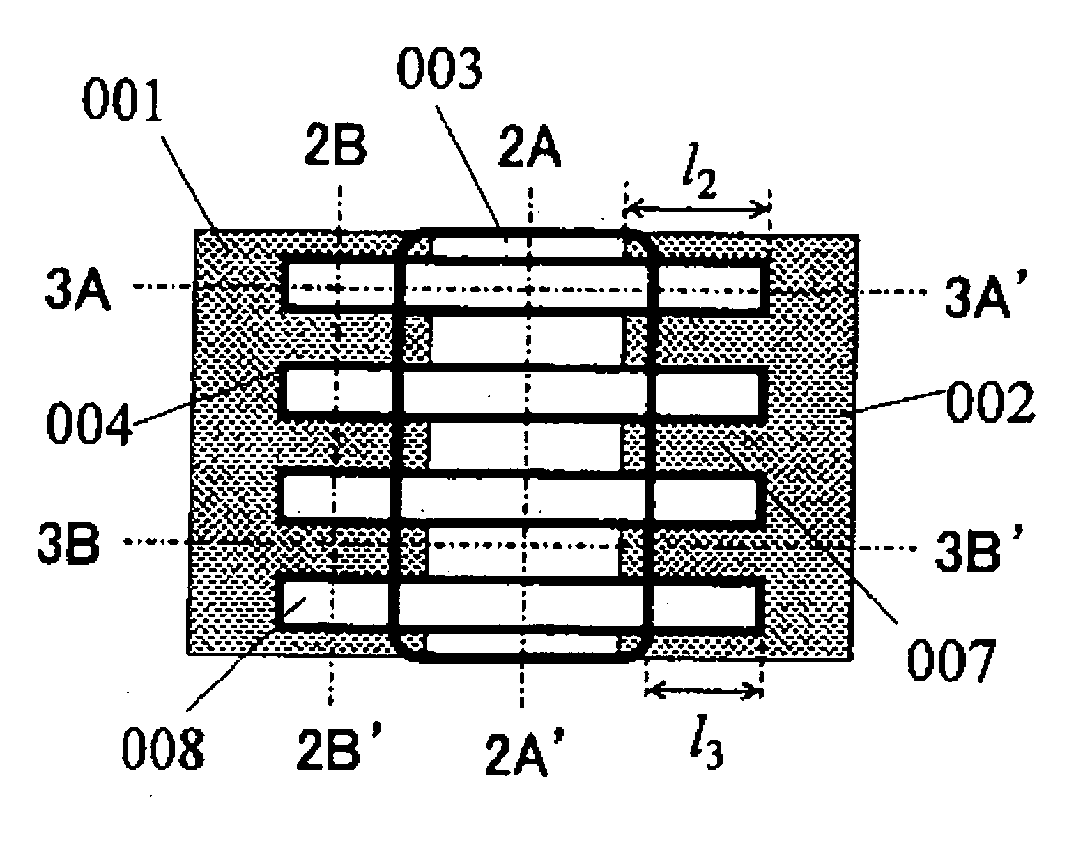
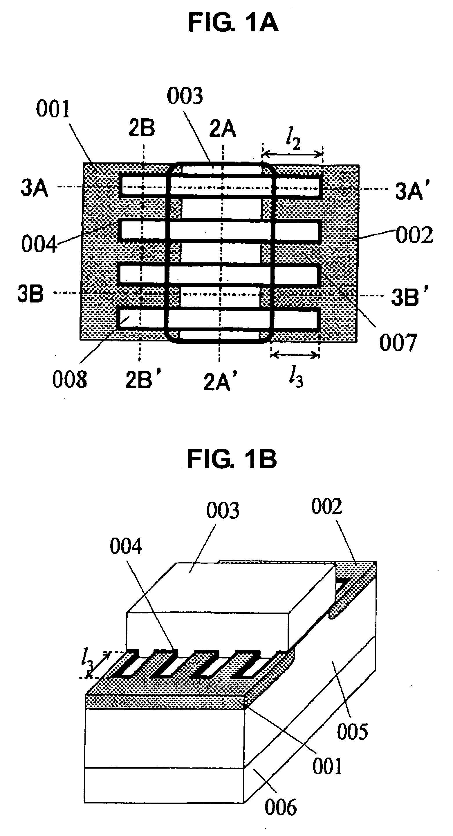
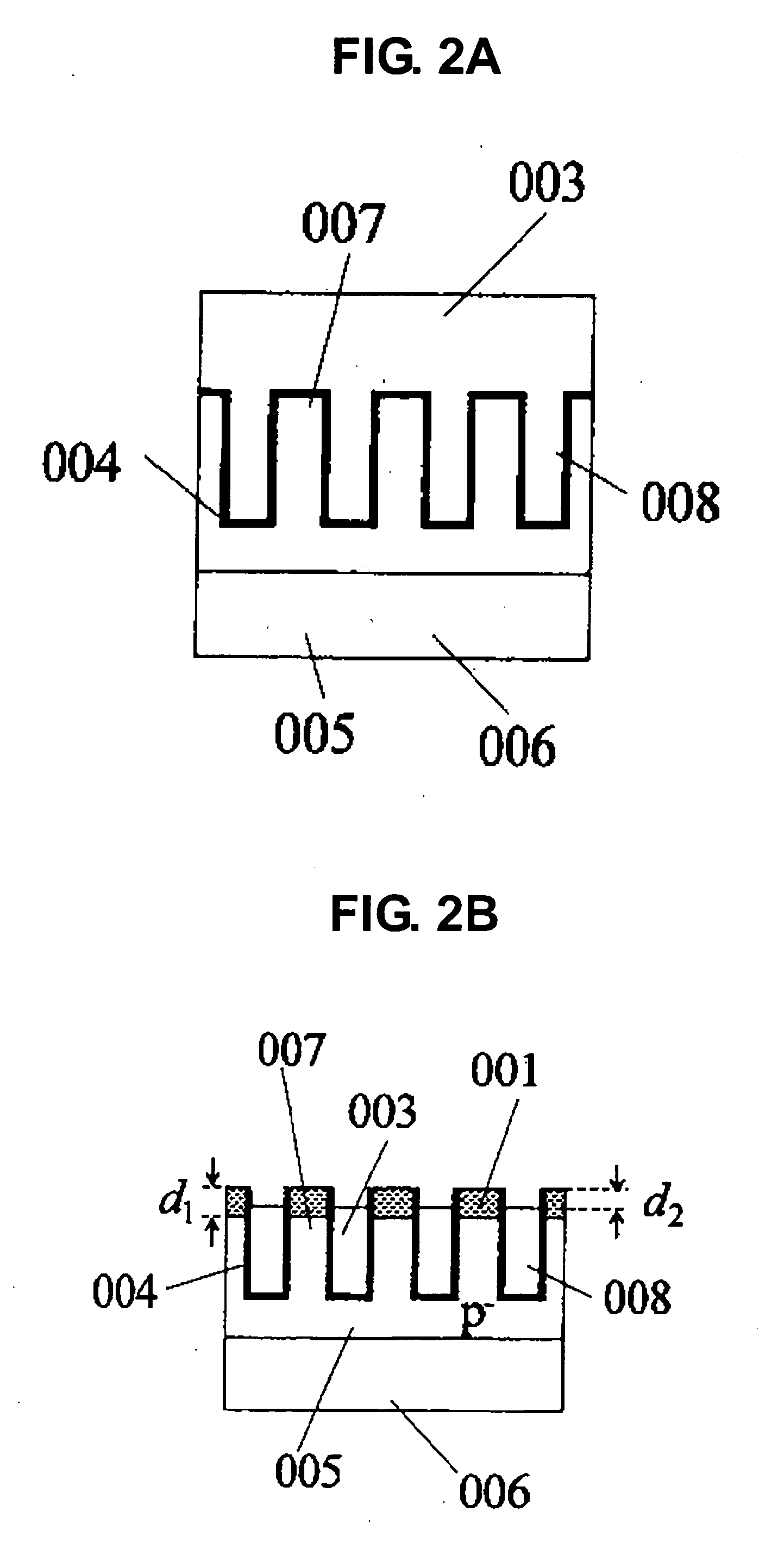
[0045]FIGS. 1A and 1B each show a representative embodiment of the present invention. FIG. 1A is a plan view of the invention, and FIG. 1B is a bird's-eye view of FIG. 1A. Referring to FIG. 1A, for convenience in viewing, a gate electrode 003 and a gate insulating film 004 outside of trenches are made transparent. A bold line indicates an edge of the gate electrode 003. Also, FIG. 2A is a cross sectional view taken along the line 2A-2A′ of FIG. 1A, FIG. 2B is a cross sectional view taken along the line 2B-2B′ of FIG. 1A, FIG. 3A is a cross sectional view taken along the line 3A-3A′ of FIG. 1A, and FIG. 3B is a cross sectional view taken along the line 3B-3B′ of FIG. 1A. In the conventional example shown in FIG. 4, the gate electrode 003 covers an entire trench portion. On the contrary, in the present invention shown in FIGS. 1 to 3, portions in a vicinity of both ends of the trench are not covered with the gate electrode 003. In this structure, a longer 13 (a longer 12) can give a l...


PUM


Abstract

Provided is a semiconductor device having a structure in which: a well region of a high resistance p-type semiconductor is disposed in a given depth from a surface of an n-type or p-type semiconductor substrate; a plurality of trenches extend from the surface of the well region to a certain depth; a gate insulating film is formed on a surface of a convex/concave portion on which the trenches are formed; a gate electrode is embedded into the trenches. The semiconductor device includes: a gate electrode film that is disposed on a substrate surface in contact with the gate electrode embedded into the trenches in the convexo-concave portion region except for a portion in the vicinity of both ends of the trenches; and a source region and a drain region that are two low resistance n-type semiconductor layers which are disposed shallower than the depth of the well region in the well region except for a lower portion of the gate electrode film.

Description

BACKGROUND OF THE INVNETION [0001] 1. Field of the Invention [0002] The present invention relates to a semiconductor device for which high driving performance is required. [0003] 2. Description of the Related Art [0004] Year by year full use of fine processing technology has enabled manufacturing of small semiconductor devices without lowering capability. This trend can also apply to a semiconductor element having high driving performance. The reduction of an ON resistance of the element per unit area has been achieved with the best use of fine processing technology. However, it is also a fact that lowering of withstanding voltage, which is caused by miniaturization of elements, hinders further improvement of the driving performance. Elements with various structures have been proposed in order to eliminate the trade-off between miniaturization and withstanding voltage. A trench gate MOS transistor is an example in a power MOS. FET with a high withstanding voltage and high driving pe...

Claims


Application Information

Patent Timeline
Patent Type & Authority Applications(United States)
IPC IPC(8): H01L21/8234
CPCH01L21/28114H01L29/0692H01L29/0869H01L29/0886H01L29/4236H01L29/785H01L29/66803H01L29/7825H01L29/7834H01L29/7835H01L29/66621H01L21/18
Inventor RISAKI, TOMOMITSU
Owner ABLIC INC
Why Eureka
Try Eureka