Method of manufacture of semiconductor device and conductive compositions used therein

a semiconductor and semiconductor technology, applied in the direction of semiconductor/solid-state device details, non-metal conductors, conductors, etc., can solve the problems of poor dispersion inside the electrode, electrodes that exhibit inadequate adhesive strength (tensile strength),

Inactive Publication Date: 2006-10-19
EI DU PONT DE NEMOURS & CO
View PDF6 Cites 101 Cited by
  • Summary
  • Abstract
  • Description
  • Claims
  • Application Information

AI Technical Summary

Problems solved by technology

Shuichi et al. teaches that powders having an average particle size of less than 0.1 μm will have poor dispersibility inside the electrode, and the electrode will exhibit inadequate adhesive strength (tensile strength).

Method used


Image

  • Method of manufacture of semiconductor device and conductive compositions used therein
  • Method of manufacture of semiconductor device and conductive compositions used therein

Examples


examples

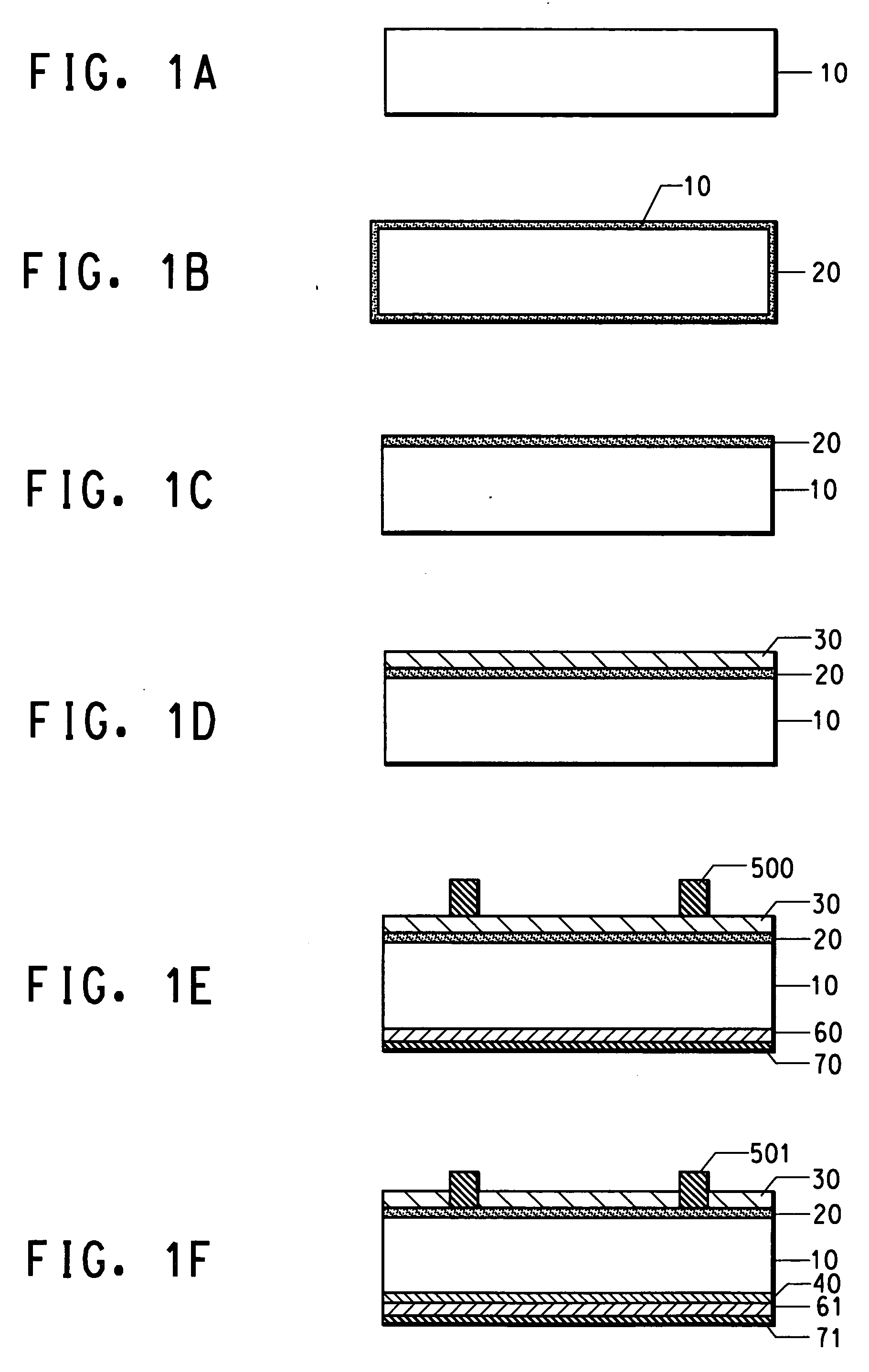
[0058] The thick film composition(s) of the present invention are described herein below in Examples 1-25.

Glass Preparation:

[0059] The glass composition(s) utilized in the Examples are detailed below in Table 2 and identified in Table 3.

TABLE 2Glass Compositions in Weight Percent of Total Glass CompositionASTMTMAGlass Composition in Weight PercentSofteningOnsetSiO2Na2OLi2OBi2O3CeO2Al2O3PbOB2O3TiO2ZnOPt. (° C.)(° C.)Glass I28.004.7055.908.103.30600502Glass II6.0080.5012.001.50430365Glass III1.641.7385.7610.86362322Glass IV9.101.4077.012.50395361Glass V1.7782.328.731.186.00—340Glass VI1.501.01.081.500.1014.90——

Paste Preparation:

[0060] Paste preparations were, in general, accomplished with the following procedure: The appropriate amount of solvent, medium and surfactant was weighed then mixed in a mixing can for 15 minutes, then glass frits and metal additives were added and mixed for another 15 minutes. Since Ag is the major part of the solids of the present invention, It was a...


PUM

PropertyMeasurementUnit
particle sizeaaaaaaaaaa
softening pointaaaaaaaaaa

Abstract

The present invention is directed to a thick film conductive composition comprising: (a) electrically conductive silver powder; (b) Zn-containing additive wherein the particle size of said zinc-containing additive is in the range of 7 nanometers to less than 100 nanometers; (c) glass frit wherein said glass frit has a softening point in the range of 300 to 600° C.; dispersed in (d) organic medium. The present invention is further directed to a semiconductor device and a method of manufacturing a semiconductor device from a structural element composed of a semiconductor having a p-n junction and an insulating film formed on a main surface of the semiconductor comprising the steps of (a) applying onto said insulating film the thick film composition as describe above; and (b) firing said semiconductor, insulating film and thick film composition to form an electrode.

Description

FIELD OF THE INVENTION [0001] This invention is directed primarily to a silicon semiconductor device. In particular, it is directed to a conductive silver paste for use in the front side of a solar cell device. TECHNICAL BACKGROUND OF THE INVENTION [0002] The present invention can be applied to a broad range of semiconductor devices, although it is especially effective in light-receiving elements such as photodiodes and solar cells. The background of the invention is described below with reference to solar cells as a specific example of the prior art. [0003] A conventional solar cell structure with a p-type base has a negative electrode that is typically on the front-side or sun side of the cell and a positive electrode on the backside. It is well-known that radiation of an appropriate wavelength falling on a p-n junction of a semiconductor body serves as a source of external energy to generate hole-electron pairs in that body. Because of the potential difference which exists at a p...

Claims


Application Information

Patent Timeline
Patent Type & Authority Applications(United States)
IPC IPC(8): H01B1/12
CPCC03C3/064Y02E10/50C03C3/0745C03C8/10C03C8/12C03C8/14C03C8/16C03C8/18C03C8/20C03C14/006C03C2214/08C03C2214/16H01B1/22H01L31/022425H05K1/092C03C3/072H01L23/48
Inventor WANG, YUELIYOUNG, RICHARD JOHN SHEFFIELDCARROLL, ALAN FREDERICKHANG, KENNETH WARREN
Owner EI DU PONT DE NEMOURS & CO
Why Eureka
Try Eureka