Gunn diode

a diode and gunn technology, applied in the field of gunn diodes, can solve problems such as the formation of domain “bunches”

Inactive Publication Date: 2006-10-19
E2V TECH (UK) LTD
View PDF6 Cites 4 Cited by
  • Summary
  • Abstract
  • Description
  • Claims
  • Application Information

AI Technical Summary

Benefits of technology

[0012] The invention permits the current flow area available for the d.c. component of the current through the Gunn diode to be restricted to a much greater extent than that for the harmonic frequency component, as a result of the skin effect.

Problems solved by technology

Electrons raised to a higher potential level have reduced mobility and travel at a slower rate, causing the formation of the domain “bunches”.
However, the Applicants have appreciated that the current density is not uniformly distributed over the cross-sectional area of the diode, because of the skin effect. FIG. 3 is a graph of current density against depth into the surface of the Gunn diode, taken through the transit region.

Method used


Image

  • Gunn diode
  • Gunn diode
  • Gunn diode

Examples


Embodiment Construction

[0032] Like parts are given like reference numerals through all the drawings.

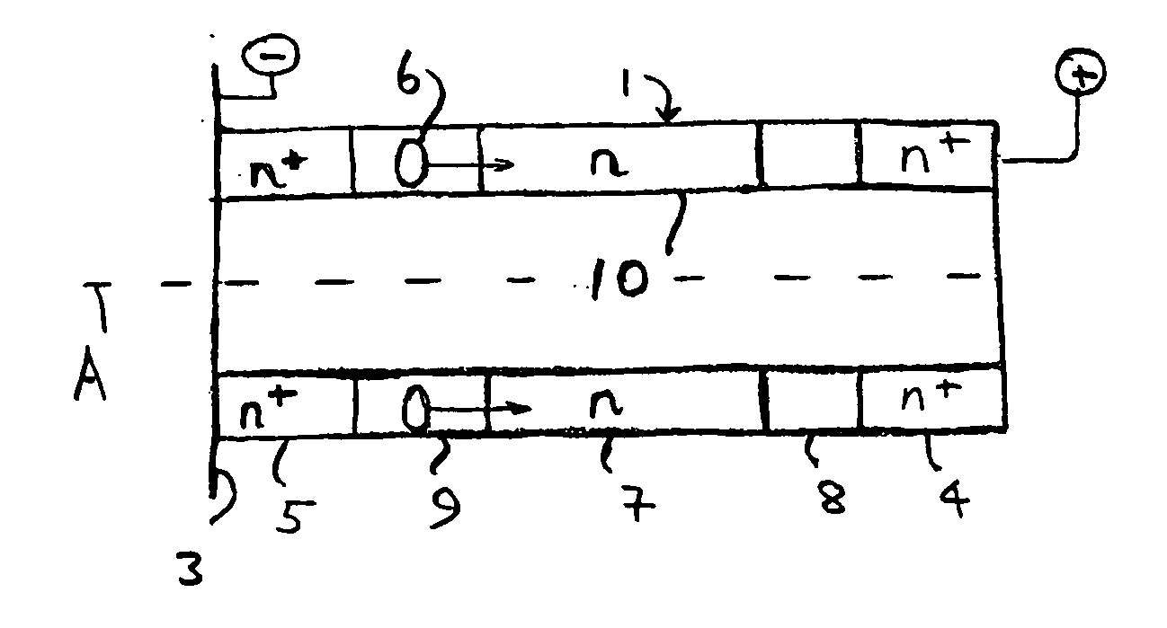
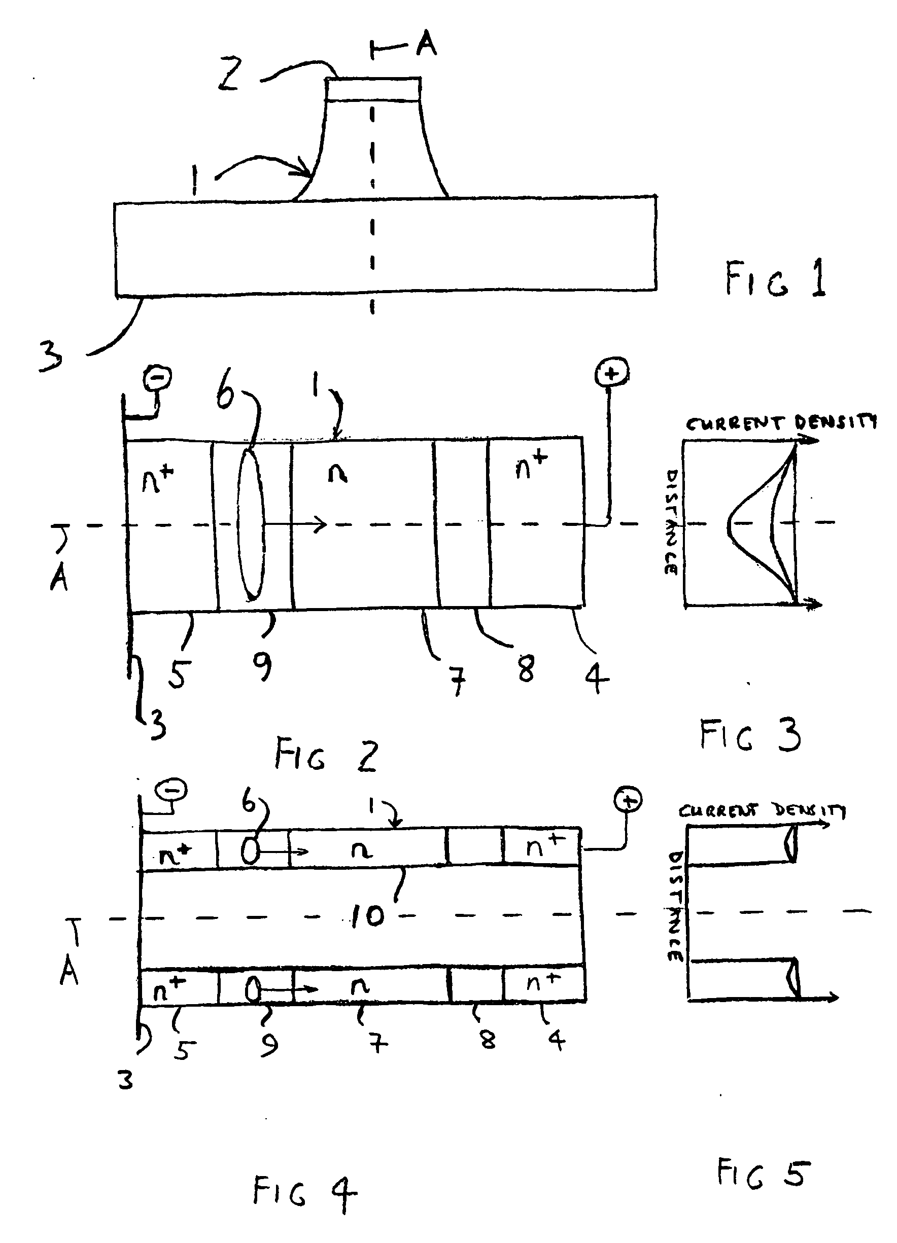
[0033] Referring to FIG. 4 of the accompanying drawings, the first Gunn diode comprises a gallium arsenide elongate portion 1 having the same tapered external shape as the known Gunn diode shown in FIG. 1 and the same doped layers 4, 5, 7 to 9 as shown in the simplified drawing of FIG. 2. Also, the Gunn diode of FIG. 4 has top 2 and bottom 3 gold contacts at its ends (not shown in FIG. 4 but shown in FIG. 13), the bottom contact forming a heat sink.

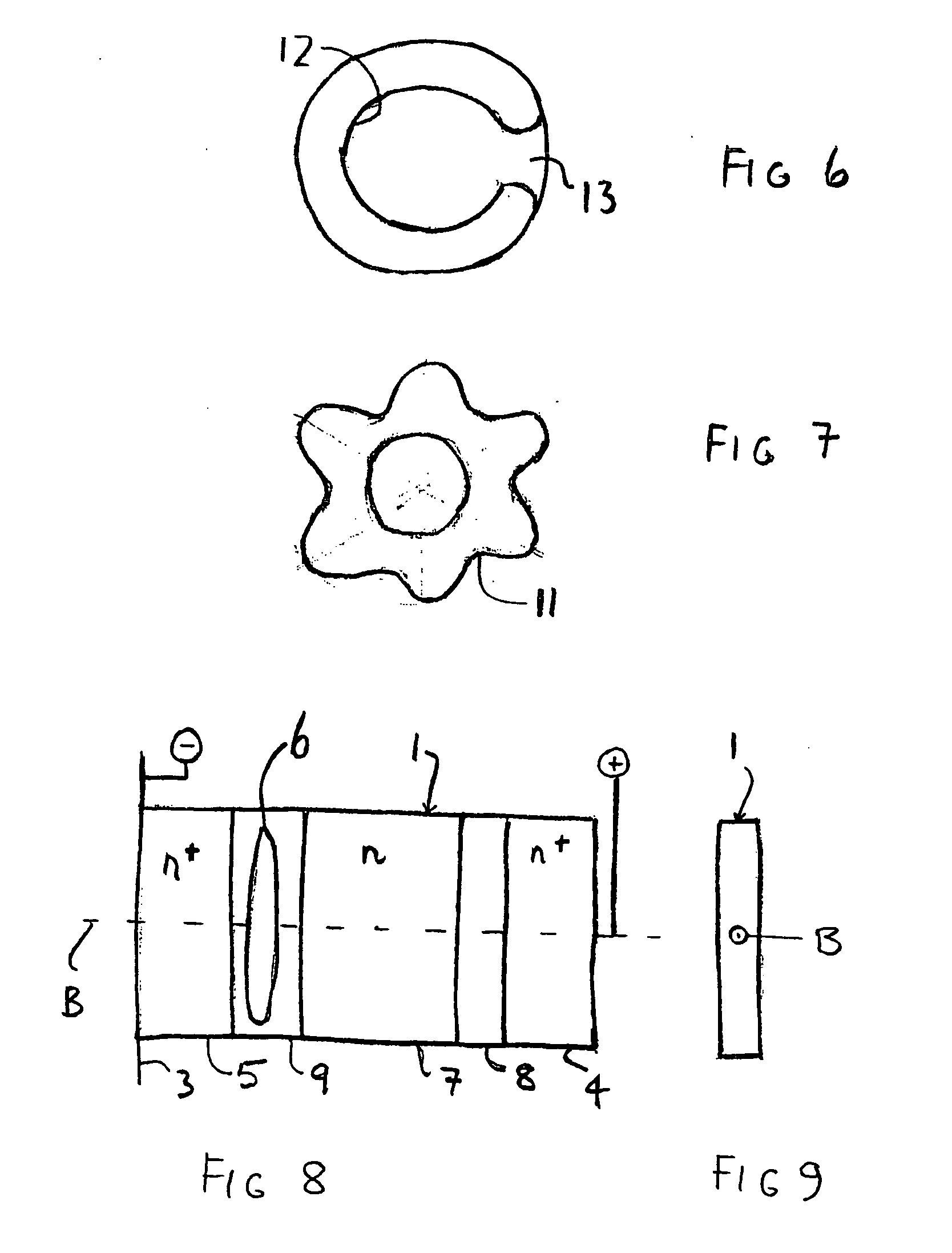
[0034] The core 10 of the Gunn diode is non-conducting. The effect of this, compared to the known Gunn diode of FIG. 2, is that the conducting area is annular, that is, ring-like, along the length of the elongate portion 1. The space charge (domain) 6 which drifts through the transit region 7 is shaped like a torus.

[0035] The central core is rendered non-conducting by implant isolation (ion implantation), that is, by bombardment of the elongate portion 1 with ...


PUM


Abstract

A Gunn diode having axis A consists of appropriately doped layers which, when a suitable voltage is applied, cause a space charge 6 to traverse a transit region 7 at a microwave frequency. In a typical known Gunn diode, the layers 4, 5 and 7 to 9 extend across the full diameter of the diode, and the space charge 6 is usually depicted as being disc-shaped. There is the disadvantage that the d.c. component of the Gunn effect current associated with a desired harmonic frequency causes undesirable heating. According to the invention, the area through which the current can flow through the elongate structure is tailored to favour the harmonic over the d.c. component, utilising the skin effect. Several ways of doing this are described, notably by making the core of the elongate portion non-conducting, for example, by ion implantation or by its removal by etching.

Description

CROSS-REFERENCE TO RELATED APPLICATION [0001] This application claims the priority of British Patent Application No. 0506588.3 filed on Mar. 31, 2005, the subject matter of which is incorporated herein by reference. BACKGROUND OF THE INVENTION [0002] This invention relates to Gunn diodes, which are also known as transferred electron devices. [0003] Such devices are used for producing low cost and compact sources of microwave oscillations, for example, for use in radar used in automotive adaptive cruise control (A Compact 77 Ghz Transceiver Module Using G3D Diode Technology for Automotive Applications, by Nigel Priestley and Brian Prime, Advanced Microsystems for Automotive Applications 2003, edited by Jurgen Valldorf and Wolfgang Gessner, Springer (ISBN 3-540-00597-8). [0004]FIG. 1 is a sectional view through the axis A of a known Gunn diode, the diode being symmetrical about its axis. The diode consists of a mass indicated generally by the reference 1 of Gallium Arsenide (GaAs) san...

Claims


Application Information

Patent Timeline
Patent Type & Authority Applications(United States)
IPC IPC(8): H03B9/12H01L47/02
CPCH01L47/026H10N80/107
Inventor NEWSOME, KEITH DAVID
Owner E2V TECH (UK) LTD
Why Eureka
Try Eureka