Non-volatile memory and fabricating method thereof

Active Publication Date: 2006-10-19
POWERCHIP SEMICON MFG CORP
View PDF2 Cites 34 Cited by
  • Summary
  • Abstract
  • Description
  • Claims
  • Application Information

AI Technical Summary

Benefits of technology

[0010] Accordingly, at least one objective of the present invention is to provide a method of fabricating a non-volatile memory that can

Problems solved by technology

Since doped polysilicon has a higher resistance, the operating speed of the device is limited that it is difficult to use the device in a high-speed en

Method used


Image

  • Non-volatile memory and fabricating method thereof
  • Non-volatile memory and fabricating method thereof
  • Non-volatile memory and fabricating method thereof

Examples


Embodiment Construction

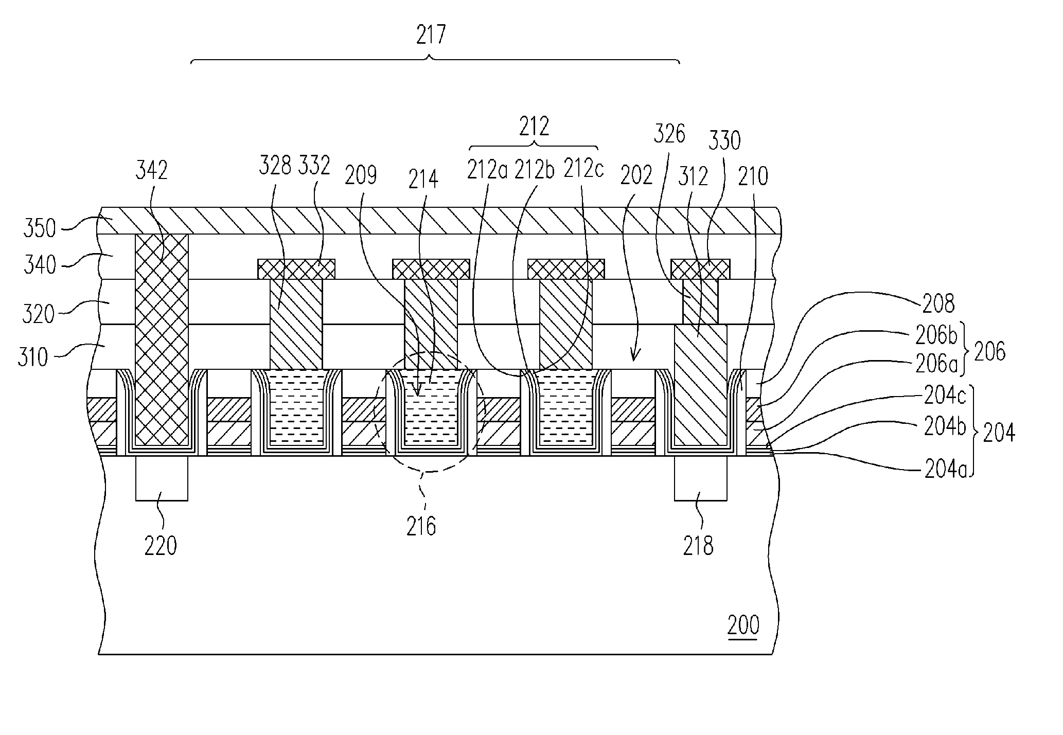
[0032] Reference will now be made in detail to the present preferred embodiments of the invention, examples of which are illustrated in the accompanying drawings. Wherever possible, the same reference numbers are used in the drawings and the description to refer to the same or like parts.

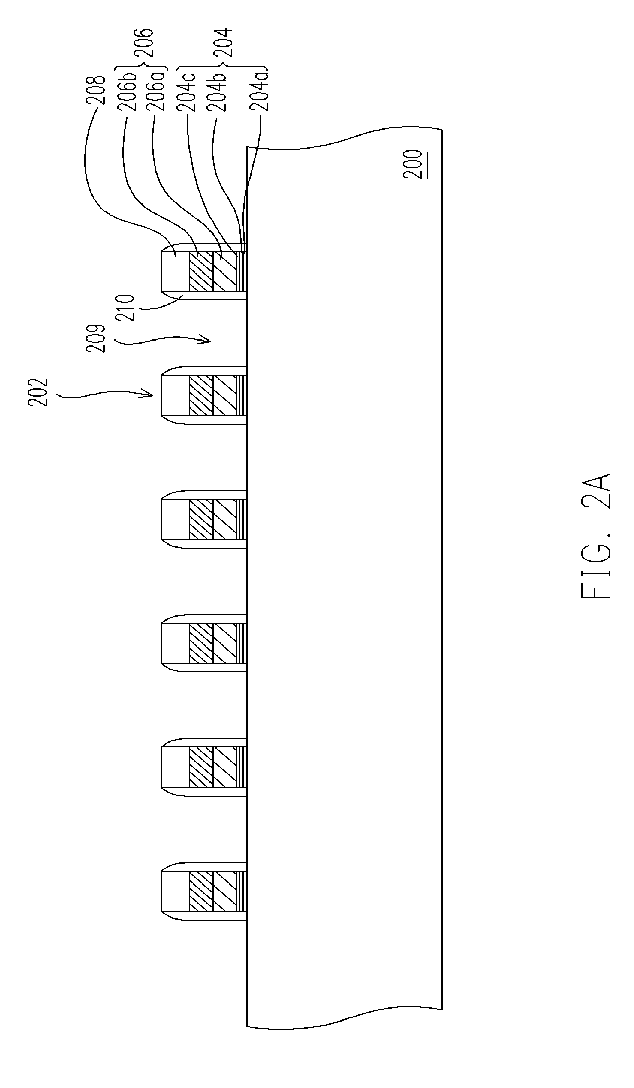
[0033]FIGS. 2A through 2E are schematic cross-sectional views showing the steps for fabricating a non-volatile memory according to one preferred embodiment of the present invention.

[0034] As shown in FIG. 2A, a substrate 200 is provided. Then, a plurality of memory units 202 is formed on the substrate 200. The memory units 202 are separated from one another by a gap 209. Each memory unit 202 includes a composite layer 204, a gate 206 and a cap layer 208 sequentially formed over the substrate 200. The memory units 202 are formed, for example, by depositing composite dielectric material, conductive material and insulating material over the substrate and patterning the aforementioned material layers ...


PUM


Abstract

A method of fabricating a non-volatile memory is provided. A memory cell array having first memory units and second memory units is formed on a substrate. Then, a source region and a drain region are formed in the substrate on the respective sides of the memory cell array. Next, a patterned first inter-layer insulating layer is formed on the substrate to form a first trench and a plurality of second trenches. A conductive layer is formed on the substrate to form a source line in the first trench and conductive lines in the second trenches. A second inter-layer insulating layer is formed on the substrate and then a conductive plug having contact with the drain region is formed in the second inter-layer insulating layer and the first inter-layer insulating layer. Then, a bit line having contact with the conductive plug is formed on the second inter-layer insulating layer.

Description

CROSS-REFERENCE TO RELATED APPLICATION [0001] This application claims the priority benefit of Taiwan application serial no. 94107083, filed on Mar. 9, 2005. All disclosure of the Taiwan application is incorporated herein by reference. BACKGROUND OF THE INVENTION [0002] 1. Field of the Invention [0003] The present invention relates to a semiconductor memory device. More particularly, the present invention relates to a non-volatile memory and fabricating method thereof. [0004] 2. Description of the Related Art [0005] Among various types of non-volatile memory products, electrically erasable programmable read only memory (EEPROM) is a memory device that has been widely used in personal computers and electronic equipment. Data can be stored, read out or erased from the EEPROM many times and stored data are retained even after power supplying the devices is cut off. [0006] Typically, the floating gate and the control gate of an EEPROM cell are fabricated using doped polysilicon. In the c...

Claims


Application Information

Patent Timeline
IPC IPC(8): H01L21/336
CPCH01L21/28282H01L27/115H01L29/792H01L29/66833H01L27/11568H01L29/40117H10B69/00H10B43/30
Inventor WEI, HOUNG-CHIPITTIKOUN, SAYSAMONETSENG, WEI-CHUNG
Owner POWERCHIP SEMICON MFG CORP
Why Eureka
Try Eureka