Planting process and manufacturing process for semiconductor device thereby, and plating apparatus

a manufacturing process and semiconductor technology, applied in the direction of electrical equipment, semiconductor devices, electrolysis components, etc., can solve the problems of difficult stable film formation, achieve the effects of preventing fluctuation in current density, improving the yield of plated films, and improving stability in the formation of metal films

Inactive Publication Date: 2006-10-26
RENESAS ELECTRONICS CORP
View PDF6 Cites 4 Cited by
  • Summary
  • Abstract
  • Description
  • Claims
  • Application Information

AI Technical Summary

Benefits of technology

[0019] After intense investigation for preventing fluctuation in a current density newly generated during inclined insertion of a wafer in a plating solution, the present inventors have found that fluctuation in a current density can be prevented by controlling a current on the basis of an inclination angle of the wafer from the liquid surface of the plating solution in the course of immersing a wafer, finally achieving this invention.
[0024] In the first step of the plating process of this invention, the wafer is inclined-inserted with applying the first current between the cathode electrode and the anode electrode and controlling the first current depending on an inclination angle of the surface between the plating solution and the film-formation surface of the wafer. Thus, it can effectively prevent fluctuation in a current density generated in the initial plating stage during the inclined insertion. It can, therefore, improve stability in the formation of a metal film and improve an yield of producing a plated film.
[0025] In the first step in the plating process of this invention, the first current applied between the anode electrode and the cathode electrode may be controlled, taking factors other than an inclination angle into account. For example, in the first step, the current may be controlled in the light of, in addition to an inclination angle, a speed in the direction of the normal line in the film-formation surface of the wafer and an elapsed time after the wafer contacts with the liquid. It can further reliably prevent fluctuation in a current density in the first step. Furthermore, in the first step, the first current may be controlled, neglecting fluctuation in an inclination angle within a given range.
[0028] In the manufacturing process of this invention, a metal film is formed on a wafer by the plating process as described above, so that even when forming a fine metal film pattern in a semiconductor device, defective burying of the metal film and local increase in a film thickness can be prevented, resulting in stable film formation. Thus, an yield in manufacturing a semiconductor device can be improved.
[0037] The plating apparatus according to this invention has a configuration where the wafer holding unit holds the film-formation surface at an inclined angle to the liquid surface and the controller controls a current intensity on the basis of the inclination angle. Thus, the configuration can effectively prevent fluctuation in a current density generated during inclined insertion with allowing for stably inclined-inserting the wafer.

Problems solved by technology

However, after investigating the method described in Japanese Patent Application No. 2003-129297, the present inventors have found that stable film formation is difficult in spite of prevention of bubble adherence by inclined insertion of a wafer.

Method used


Image

  • Planting process and manufacturing process for semiconductor device thereby, and plating apparatus
  • Planting process and manufacturing process for semiconductor device thereby, and plating apparatus
  • Planting process and manufacturing process for semiconductor device thereby, and plating apparatus

Examples


embodiment 1

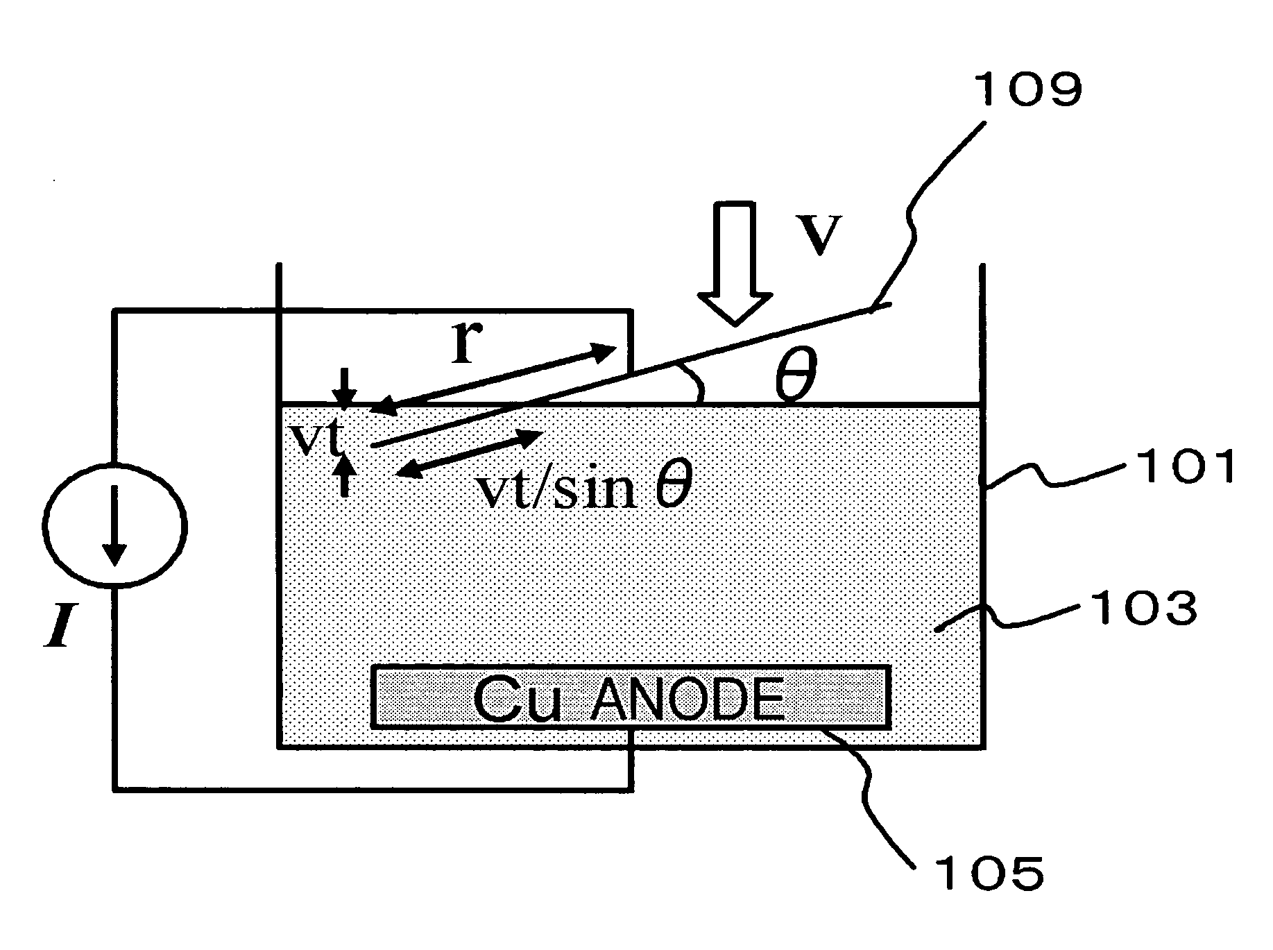
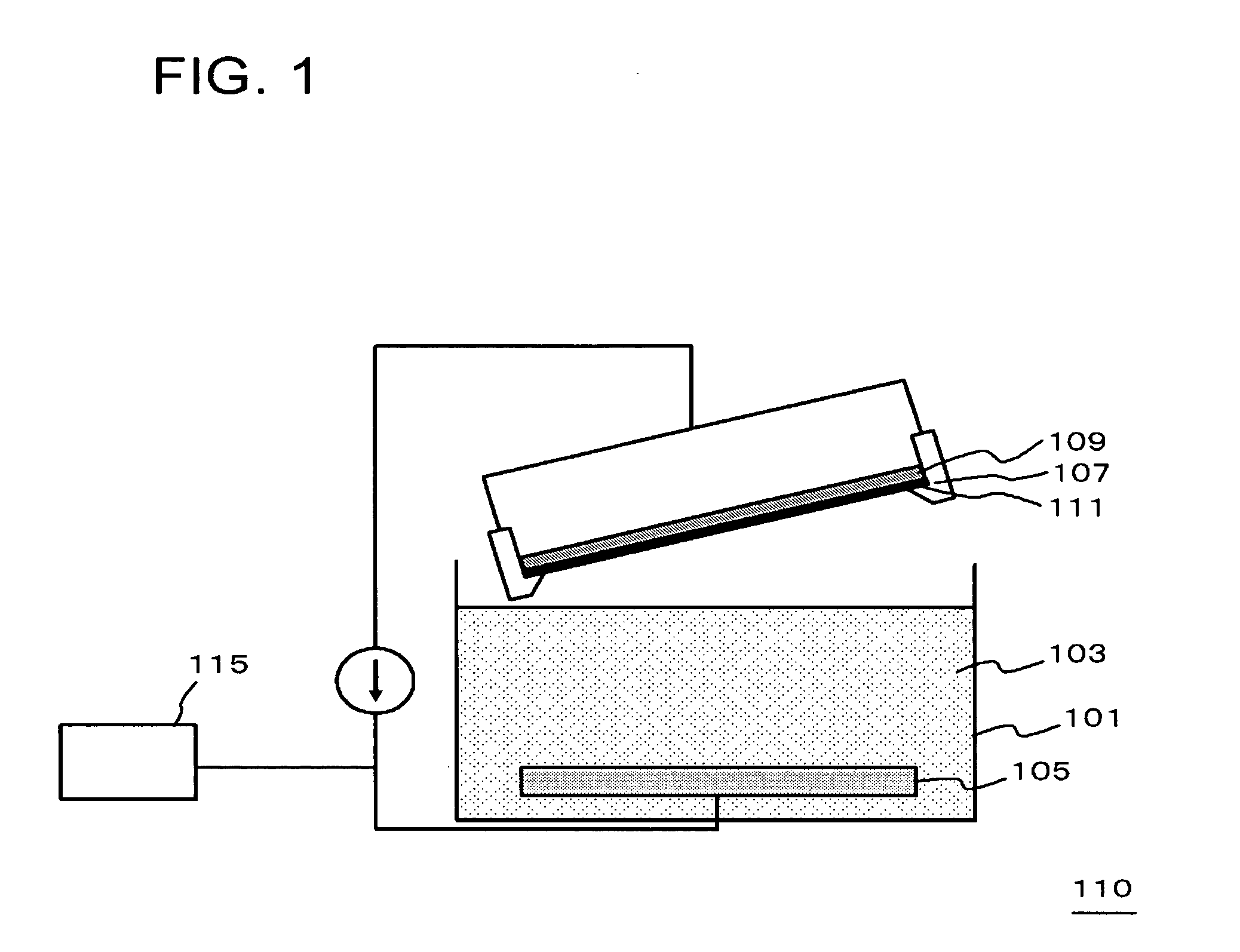
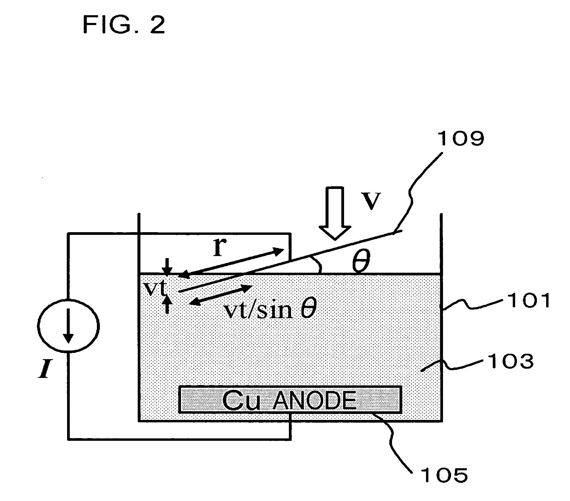
[0068]FIG. 1 is a cross-sectional view illustrating a configuration of a plating apparatus in this embodiment. The plating apparatus 110 shown in FIG. 1 has

[0069] a plating bath 101 to be filled with a plating solution 103,

[0070] a wafer moving unit (a driving unit, not shown) whereby a wafer 109 held by a cathode electrode 107 is immersed into the plating solution 103,

[0071] the cathode electrode 107 feeding a current to the wafer 109 when it comes into contact with the wafer 109,

[0072] an anode electrode (Cu anode electrode 105) disposed in the plating bath 101 such that it faces the cathode electrode 107,

[0073] a power source 115 for applying a current between the Cu anode electrode 105 and the cathode electrode 107, and

[0074] a controller 117 controlling a current intensity applied between the Cu anode electrode 105 and the cathode electrode 107 on the basis of an inclination angle of the film-formation surface from the liquid surface (FIG. 5). The cathode electrode 107 ac...

embodiment 2

[0109] This embodiment relates to another process for controlling a current applied between a cathode electrode and an anode electrode in electrolytic plating using the plating apparatus 110. In embodiment 1, a current intensity applied between a cathode electrode and an anode electrode is controlled in accordance with the above equation (1) in step 101 in forming a plating film. In this embodiment, the wafer 109 is immersed into the plating solution at a substantially constant speed while a current intensity applied between the electrodes is varied in proportion to an elapsed time t after the wafer 109 contacts with the plating solution 103 in step 101.

[0110] Specifically, in step 101 described above in embodiment 1, a current intensity I represented by the following equation (2) instead of equation (1) is applied.

I=I0t / t0  (2)

[0111] wherein I0 is an intensity of the second current and t0 is a time of completion of the first step.

[0112] More specifically, in this embodiment, θ ...

embodiment 3

[0116] This embodiment relates to another process for controlling a current applied between a cathode electrode and an anode electrode in electrolytic plating using the plating apparatus 110. Although there has been described immersion with a constant inclination angle θ of the wafer 109 from the plating solution 103 in embodiments 1 and 2 as examples, an inclination angle θ may be a time-dependent variable.

[0117]FIGS. 9, 10A, 10B, 11A, 11B and 12 illustrate a plating process using the plating apparatus 110. FIG. 9 is a plane view illustrating immersion of the wafer 109 into the plating solution 103. FIGS. 10A, 10B, 11A, 11B and 12 are cross-sectional views illustrating immersion of the wafer 109 into the plating solution 103. FIG. 13 shows relationship between an elapsed time after the wafer 109 contacts with the plating solution 103 and a current intensity I applied between the Cu anode electrode 105 and the cathode electrode 107 in the plating apparatus 110.

[0118] As shown in F...


PUM

PropertyMeasurementUnit
constant voltageaaaaaaaaaa
voltageaaaaaaaaaa
voltageaaaaaaaaaa

Abstract

An objective of this invention is to reliably form a plating film. The following two steps are sequentially conducted: step 101 of connecting a film-formation surface of a wafer 109 to a cathode electrode 107, making the film-formation surface inclined from the surface of a plating solution 103 and immersing the wafer 109 into the plating solution 103 with applying a first current between the cathode electrode 107 and an Cu anode electrode 105 disposed in the plating solution 103, and step 103 of, after immersing the film-formation surface in the plating solution 103, applying a second current between the cathode electrode 107 and the Cu anode electrode 105 to form a metal film on the film-formation surface by electrolytic plating. In step 101, the first current is controlled on the basis of an inclination angle between the liquid surface and the film-formation surface.

Description

[0001] This application is based on Japanese patent application NO. 2005-125782, the content of which is incorporated hereinto by reference. BACKGROUND [0002] 1. Technical Field [0003] This invention relates to a plating process for forming a conducting film by electrolytic plating and a process for manufacturing a semiconductor device by the plating process, as well as a plating apparatus. [0004] 2. Related Art [0005] A damascene process is one of processes for forming a Cu multilayer interconnection in an LSI. In a damascene process, a monolayer or multilayer insulating film is formed on an Si wafer with a transistor, and the insulating film is selectively removed to form a trench of an interconnection pattern and a hole called as a via for electrical connection between multilayer interconnection layers. Next, a material containing a high-melting metal called as a barrier metal is deposited by chemical vapor deposition or physical vapor deposition. Then, a Cu film called as a seed...

Claims


Application Information

Patent Timeline
Patent Type & Authority Applications(United States)
IPC IPC(8): C25D5/00
CPCC25D5/00C25D5/18H01L21/2885C25D17/001H01L21/76877C25D7/123H01L21/76849
Inventor FURUYA, AKIRATSUCHIYA, YASUAKI
Owner RENESAS ELECTRONICS CORP
Why Eureka
Try Eureka