Pattern defect inspection method and apparatus

a pattern and defect technology, applied in the field of pattern defect inspection methods and apparatuses, can solve the problems of data processing, false defect generation, and increased workload, and achieve the effects of high detection sensitivity, high accuracy, and reduced workload

Inactive Publication Date: 2006-10-26
KK TOPCON
View PDF0 Cites 44 Cited by
  • Summary
  • Abstract
  • Description
  • Claims
  • Application Information

AI Technical Summary

Benefits of technology

[0030] In a second mode according to the invention, a circuit design pattern graphic of the device is used as the design data of a die-to-database inspection. Generally, in order to correct an optical limit of the stepper, the optical proximity effect correction pattern is often added in producing the photomask. In the second mode, it is assumed that the design data of the pattern is compared to the obtained image to perform the inspection by using the design pattern in which the ideal pattern to be formed on the wafer is described. The stepper optical proximity effect correction pattern actually used in forming the pattern of the photomask on the wafer is not added to the ideal pattern. The design data is similarly converted into the wafer image formed with the stepper by the proper computing formula, the obtained image actually measured is simultaneously converted into the wafer image by the similar method, and the defect is detected by comparing the design data and the obtained image. In the first mode, when an error exists in the OPC pattern design, there is a drawback that the defect is not found even if the comparison is performed based on the design data. Accordingly, it is necessary that the inspection be performed with the original design data to which the pattern with OPC is not added. In this case, even if the computing formula for making the wafer image from the design data of the second embodiment is similar to that of the first embodiment, it is obvious that different parameters are used in the second mode. On the other hand, in the second mode, the method of determining the wafer image from the obtained image is similar to that of the first mode.
[0031] In a third mode according to the invention, the inspection is performed with the two above-described pieces of design data as the design data of die-to-database inspection. That is, the two pieces of design data include the pattern data with OPC which is of the design pattern produced in making the photomask and the original design data to which the stepper optical proximity effect correction pattern is not added. The third mode is the method in which the pieces of design data are converted into the wafer image by the proper method, the wafer images are compared to each other by using the measured obtained image and three kinds of the image data, and thereby the defect is detected. In the third mode, the mistake of the pattern with OPC becomes clear by comparing the pieces of design data to each other, and whether the defect derives the mask production or from the data can be known from the measurement pattern at the same time.
[0032] A fourth mode according to the invention adopts die-to-die inspection. The method of inspecting the wafer images is also efficiently used in the case where the pattern defect formed in the measurement sample is inspected by comp

Problems solved by technology

Conventionally, because design data capacity is largely increased by particularly adding the OPC pattern, the data handling becomes worse in the inspection apparatus, and the significant burden is placed on the control circuit which generates the image from the design data in the conventional way.
The improvement of the detection sensitivity is incompatible with the decrease in false defect (the defect having no influence on the pattern formation on the wafer while regarded as the defect

Method used


Image

  • Pattern defect inspection method and apparatus
  • Pattern defect inspection method and apparatus
  • Pattern defect inspection method and apparatus

Examples


Embodiment Construction

[0050] Plural embodiments of the invention will be described below with reference to the drawings.

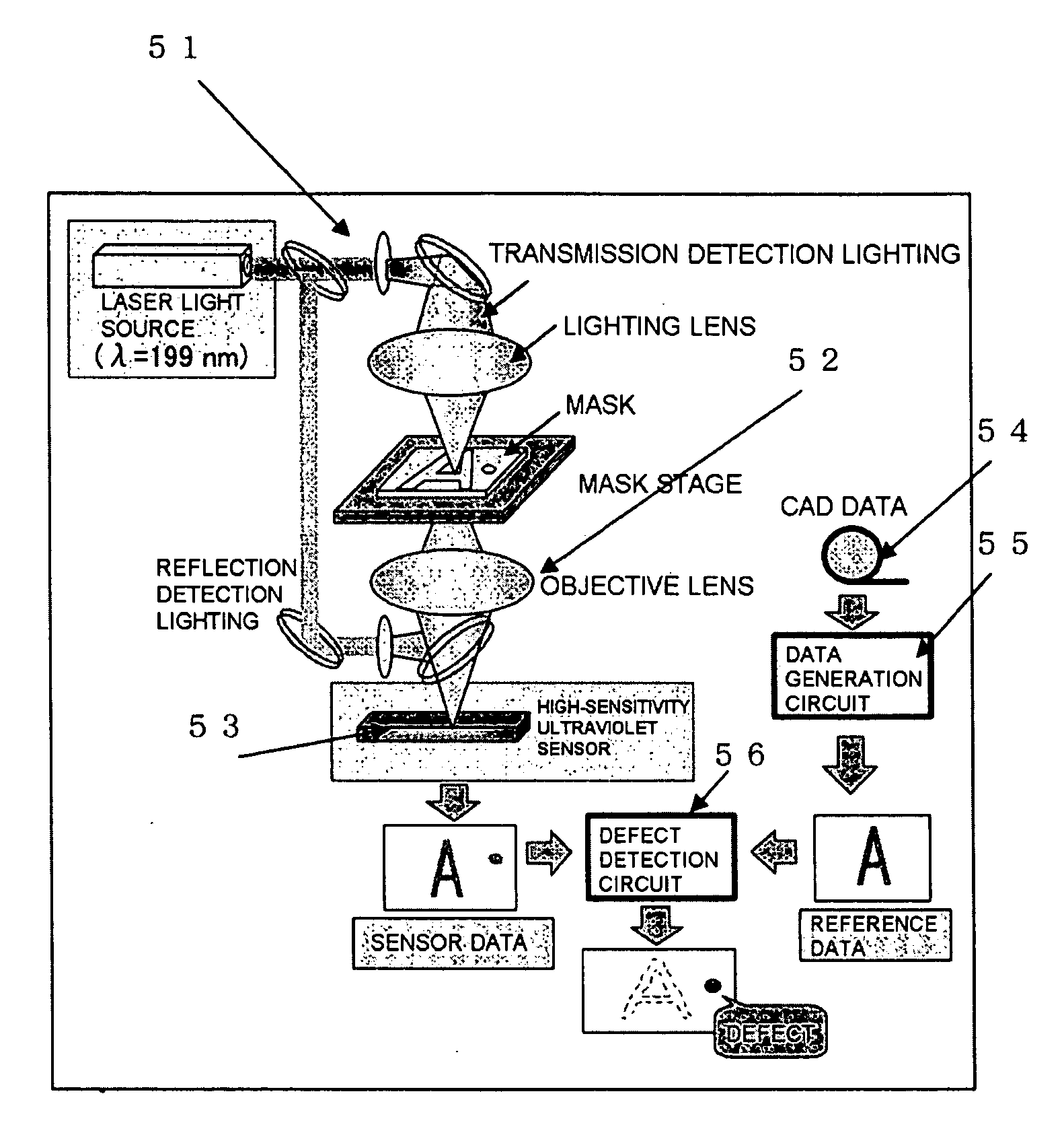
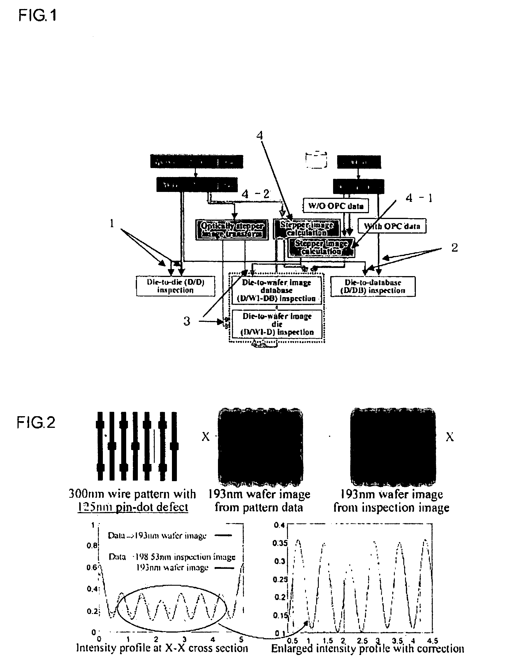
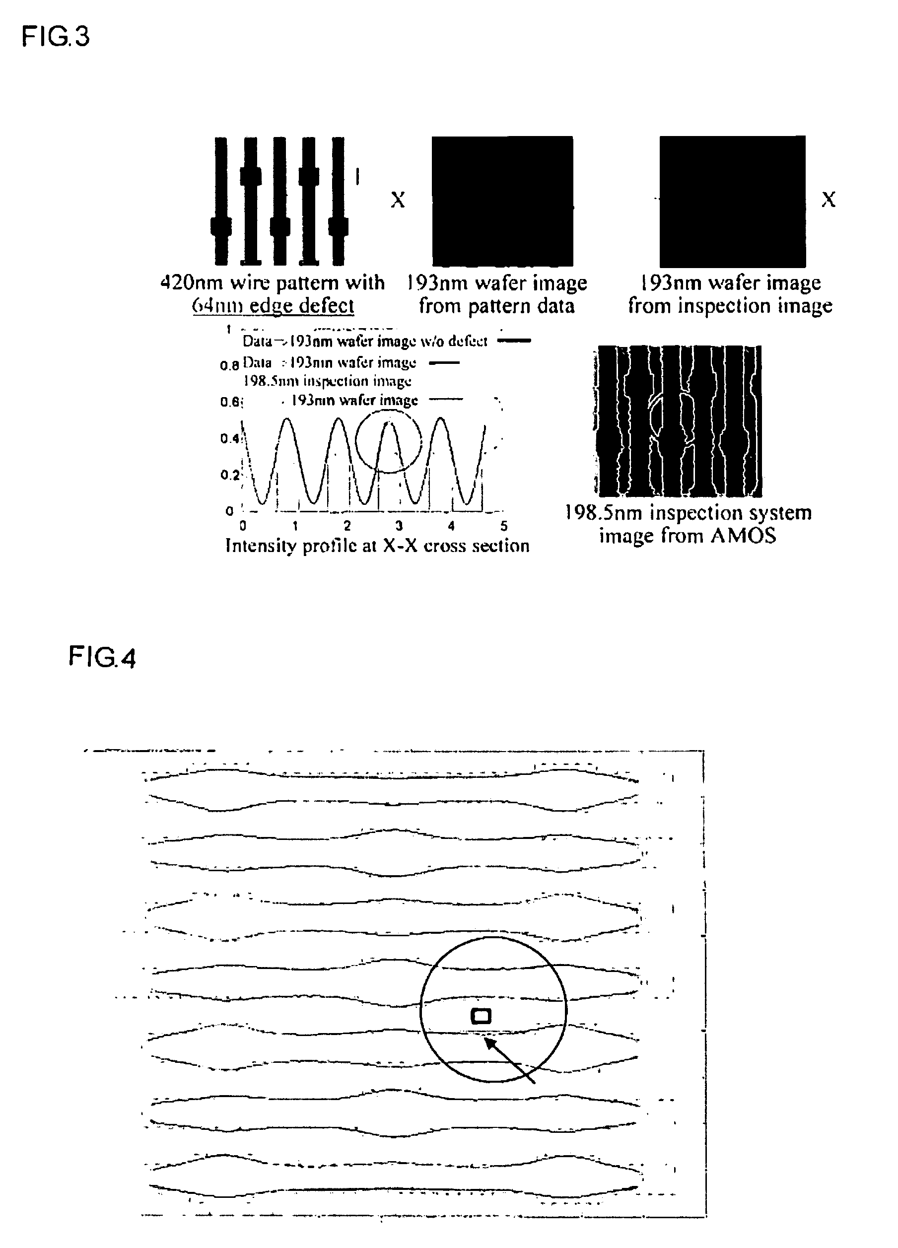
[0051]FIG. 1 shows a concept of basic inspection according to an embodiment of the invention, particularly shows an example of an inspection system diagram in a mask defect inspection apparatus.

[0052] In the case of the inspection of the images adjacent to each other (die-to-die inspection), the inspection is performed by the flow of “1” shown in FIG. 1 with respect to the image measured by the inspection apparatus. In the case where the image is compared to the design data (die-to-database inspection), the inspection is performed through a route shown by “2”, the design data is expanded to a bit image, the bit image is processed with a proper filter expressing characteristics of the inspection optical system (basically the optical system can be expressed by the filter in which inverse Fourier transform is performed to the characteristics shown by MTF) to form the image close to the m...


PUM


Abstract

A method and an apparatus for irradiating a measurement sample with an energy beam, a pattern being formed in the measurement sample, providing an optical system for detecting transmitted energy beam or reflected energy beam from the measurement sample, obtaining a pattern image, and comparing design data of the pattern and an image of the obtained image pattern to inspect a defect of the pattern formed in the measurement sample, wherein the measurement sample is a so-called photomask, a design pattern produced in producing the photomask is used as the design data of the pattern, and, in a procedure of performing inspection by comparing the obtained image and the design data, the design data is converted into an image (hereinafter referred to as wafer image) by a proper method, the wafer image being formed through a stepper used for actually forming the pattern of the photomask on a wafer, the obtained image actually measured is simultaneously converted into a wafer image by a proper method, and the defect is detected by comparing both wafer images to each other.

Description

TECHNICAL FIELD [0001] The present invention relates to a method and an apparatus for inspecting a defect or defects of a pattern, and in particular a method and apparatus for inspecting the defects formed in the patterns of a mask, a wafer substrate, or the like used in producing a semiconductor device. RELATED ART [0002] In a pattern constituting a large scale integrated circuit (LSI), a minimum dimension is reduced to the order of nanometers. One of main causes for decreasing a yield in an LSI production process are defects present in a mask which is used when an ultrafine pattern is exposed and transferred onto a semiconductor wafer by lithography. [0003] Particularly, as a pattern dimension of LSI formed on the semiconductor wafer becomes finer, the dimension of the pattern defect to be detected becomes extremely small. Therefore, development of the apparatus for inspecting the extremely small defect is actively proceeding. A configuration of the pattern defect inspection appar...

Claims


Application Information

Patent Timeline
IPC IPC(8): H04N7/18G06K9/00G06K9/62G01N21/00
CPCG01N21/95607G03F1/84G06T2207/30148G06K2209/19G06T7/001G06K9/00G06V2201/06G06F18/00
Inventor TAKADA, AKIRATOJO, TORU
Owner KK TOPCON
Why Eureka
Try Eureka