Polysilane composition, optical waveguide and method for fabrication thereof
a technology of polysilane and composition, applied in the direction of instruments, cladded optical fibres, synthetic resin layered products, etc., can solve the problems of slow optical signal transmission speed, failure to achieve uniform photobleaching, and failure to simultaneously achieve optimization of core shape and minimization of propagation loss and coupling loss, so as to achieve satisfactory core shape, reduce the refractive index of exposed regions, and improve the effect of optical signal quality
- Summary
- Abstract
- Description
- Claims
- Application Information
AI Technical Summary
Benefits of technology
Problems solved by technology
Method used
Image
Examples
example 1
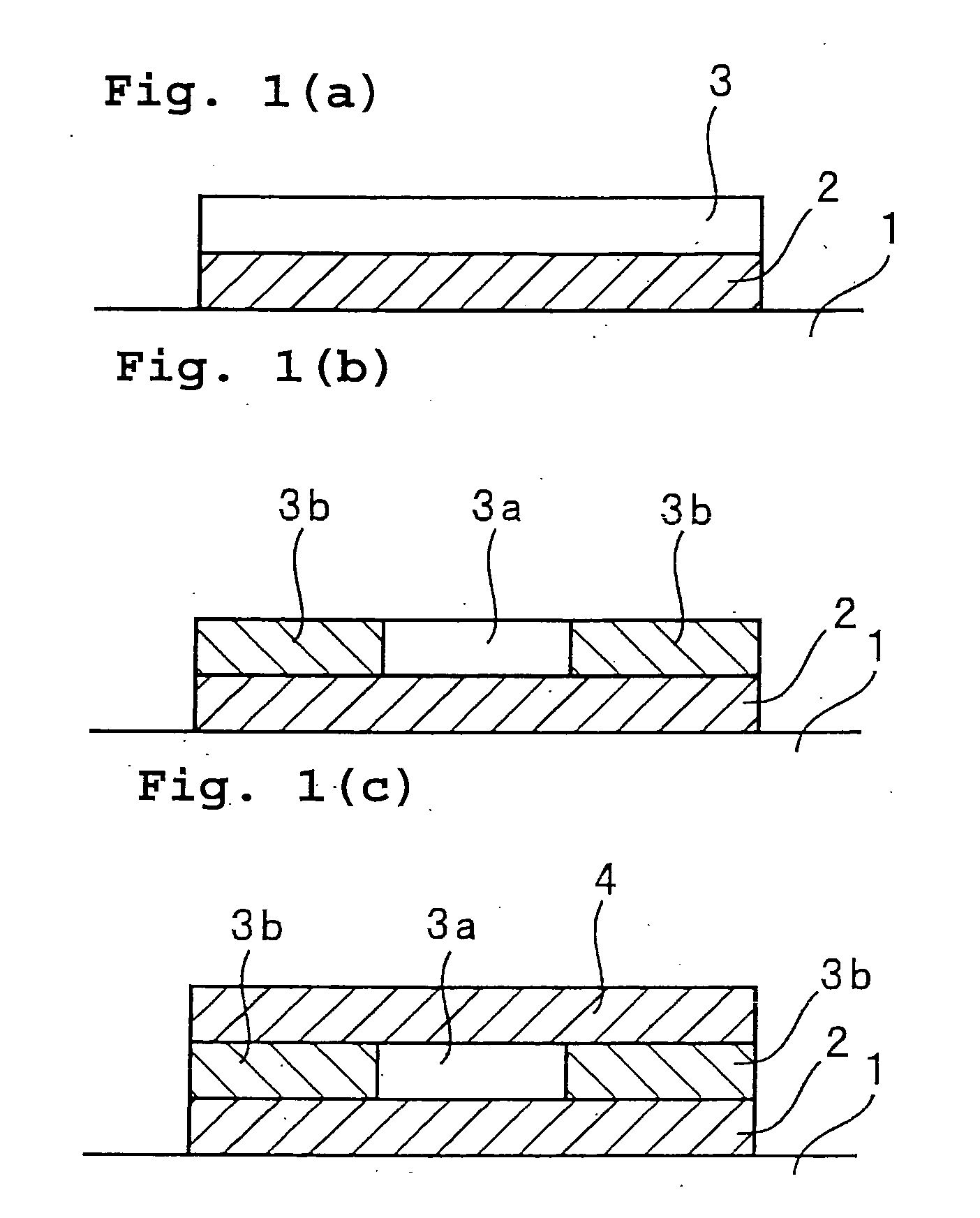
[0064] Polymer optical waveguides were fabricated according to the first aspect of the fabrication method of the present invention, as shown in FIG. 1.
[0065] As shown in FIG. 1(a), the solution for forming upper and lower claddings was spin coated onto a glass substrate 1, prebaked at 150° C. for 30 minutes and then postbaked at 200° C. for 30 minutes to form a 20 μm thick, lower cladding layer 2.
[0066] Each of the above-synthesized polysilane compositions No. 1-No. 5 was spin coated on the lower cladding layer 2 and then prebaked at 130° C. for 30 minutes to form a 50 μm thick polysilane layer 3.
[0067] The polysilane layer 3 was exposed to an ultraviolet radiation through a photomask located above its region corresponding to a core layer 3a. The ultraviolet irradiation was performed using an ultraviolet radiation of 310 nm wavelength and 15 J / cm2 radiation energy.
[0068] Thereafter, postbaking was carried out at 150° C. for 30 minutes. By this postbaking, the region correspondin...
example 2
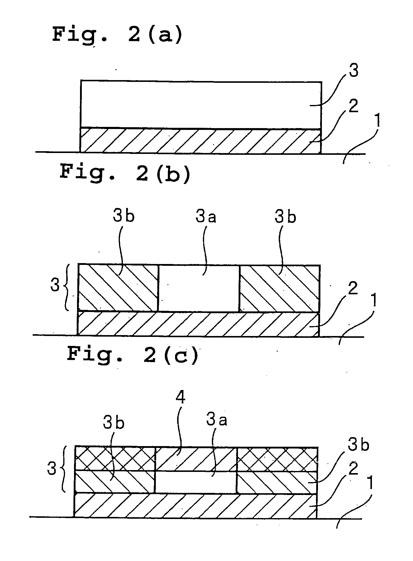
[0070] A polymer optical waveguide was fabricated according to the second aspect of the fabrication method of the present invention, as shown in FIG. 2.
[0071] As shown in FIG. 2(a), the solution for forming upper and lower claddings was spin coated onto a glass substrate 1, prebaked at 150° C. for 30 minutes and then postbaked at 200° C. for 30 minutes to form a 20 μm thick, lower cladding layer 2.
[0072] The polysilane composition No. 3 in the form of a solution was spin coated on the lower cladding layer 2 and then prebaked at 130° C. for 30 minutes to form a 70 μm thick polysilane layer 3.
[0073] The polysilane layer 3 was exposed to an ultraviolet radiation through a photomask located above its region corresponding to a core layer 3a. The ultraviolet irradiation was performed using an ultraviolet radiation of 310 nm wavelength and 15 J / cm2 radiation energy.
[0074] Thereafter, postbaking was carried out at 145° C. for 30 minutes and then at 190° C. for 5 minutes. By this postbak...
example 3
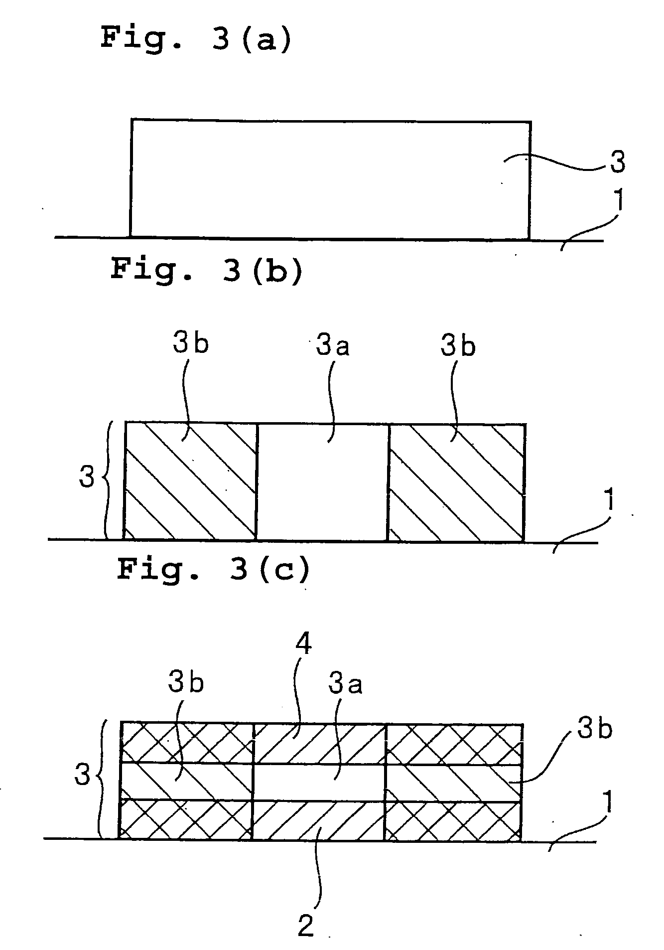
[0076] A polymer optical waveguide was fabricated according to the third aspect of the fabrication method of the present invention, as shown in FIG. 3.
[0077] As shown in FIG. 3(a), the polysilane composition No. 3 in the form of a solution was spin coated onto a glass substrate 1 and then prebaked at 130° C. for 30 minutes to form a 80 μm thick polysilane layer 3.
[0078] This polysilane layer 3 was exposed to an ultraviolet radiation through a photomask located above its region corresponding to a core layer 3a. The ultraviolet irradiation was performed using an ultraviolet radiation of 310 nm wavelength and 15 mJ / cm2 radiation energy. Subsequently, postbaking was carried out at 145° C. for 30 minutes and at 190° C. for 5 minutes. By this process, the region corresponding to a lateral cladding layer 3b was photobleached and lowered in refractive index to form the lateral cladding layer 3b, as shown in FIG. 3(b). The unexposed region was left as the core layer 3a.
[0079] After remova...
PUM
| Property | Measurement | Unit |
|---|---|---|
| thickness | aaaaa | aaaaa |
| carbon number | aaaaa | aaaaa |
| light transmittance | aaaaa | aaaaa |
Abstract
Description
Claims
Application Information


