Adiabatic rotational switching memory element including a ferromagnetic decoupling layer

a technology of ferromagnetic decoupling layer and memory element, which is applied in the direction of magnetic-field-controlled resistors, magnetic bodies, semiconductor devices, etc., can solve the problems of large memory performance, dramatic increase of antiferromagnetic coupling forces, and detrimental to down-scaling of memory cells, etc., and achieve the effect of increasing coupling energy

Inactive Publication Date: 2006-11-02
QIMONDA
View PDF4 Cites 10 Cited by
  • Summary
  • Abstract
  • Description
  • Claims
  • Application Information

AI Technical Summary

Benefits of technology

[0011] In light of the above, it is an object of the invention to provide a magnetoresistive memory element allowing a memory element size down-scale without thereb

Problems solved by technology

In view of modem portable equipment, such as portable computers, digital still cameras and the like, requiring very large memory performance, one of the most important issues for MRAM cells is a down-sizing thereof.
However, in the

Method used


Image

  • Adiabatic rotational switching memory element including a ferromagnetic decoupling layer
  • Adiabatic rotational switching memory element including a ferromagnetic decoupling layer
  • Adiabatic rotational switching memory element including a ferromagnetic decoupling layer

Examples


Embodiment Construction

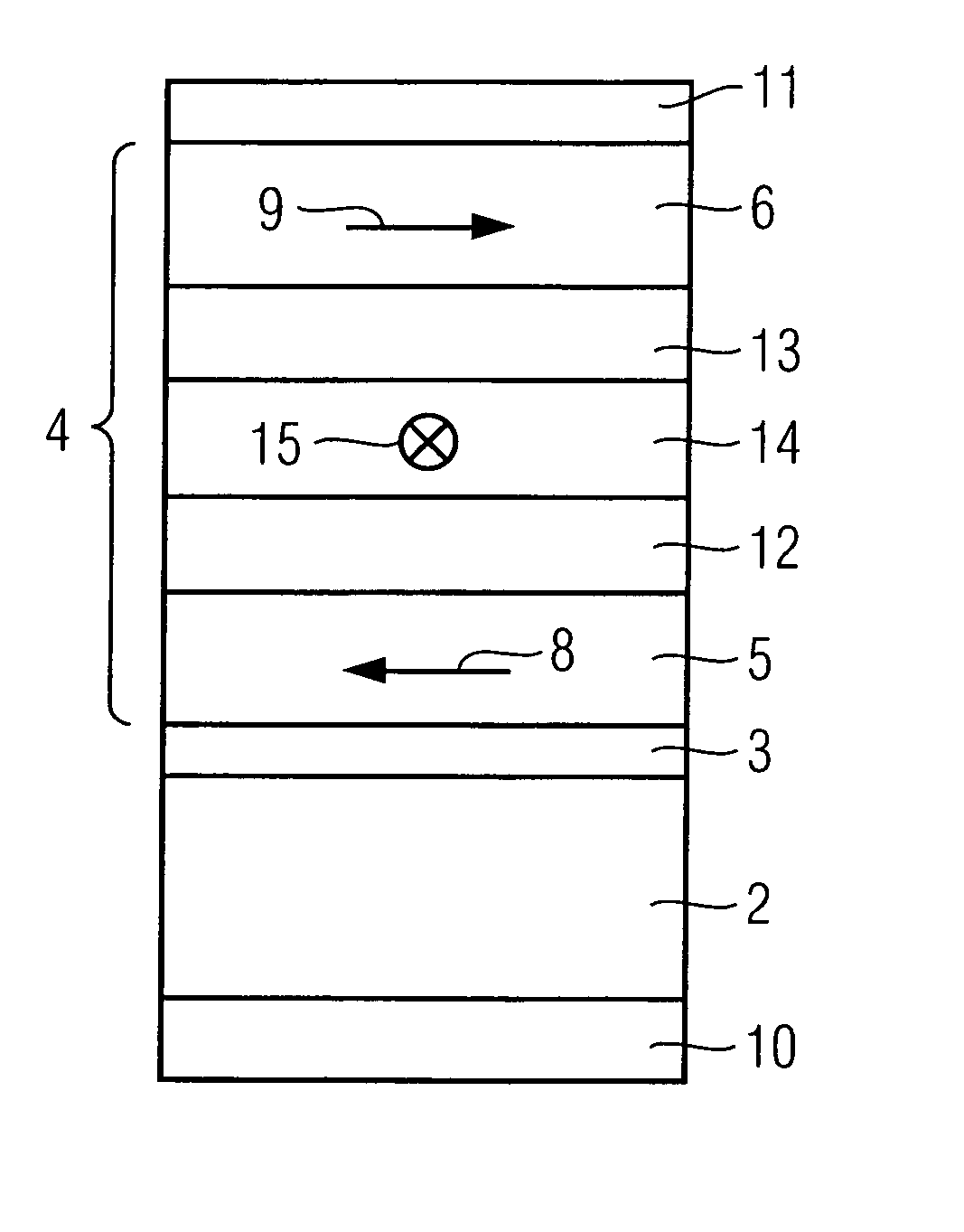
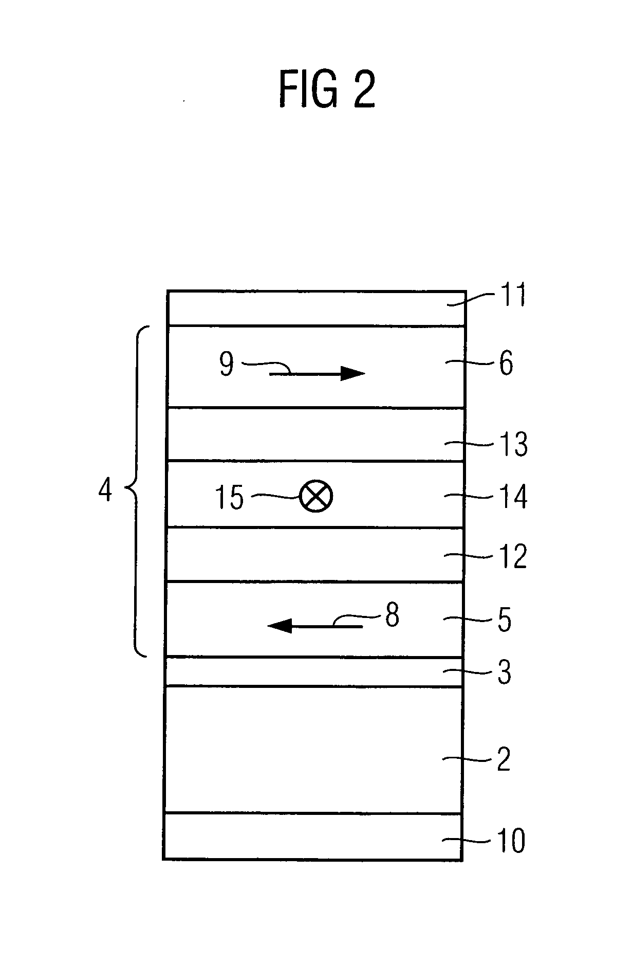
[0023] An exemplary embodiment of a memory element in accordance with the invention is depicted in FIG. 2. A patterned layered stack includes a tunneling barrier 3 including at least one tunneling barrier layer made of a non-magnetic material, a ferromagnetic reference region 2 and a ferromagnetic free region 4. The ferromagnetic reference region 2 includes a fixed magnetization arranged on one side and adjacent the tunneling barrier 3. The ferromagnetic free region 4 includes a free magnetization arranged on an opposite side and adjacent the tunneling barrier 3 and is free to be switched between oppositely aligned directions along a magnetic easy axis thereof, which typically is chosen to be in parallel alignment as to the fixed magnetization. The tunneling barrier 3 and the ferromagnetic reference and free regions 2, 4 together form a magnetoresistive tunneling junction. The ferromagnetic free region 4 includes two ferromagnetic free layers 5, 6 which are magnetically coupled. Opt...


PUM


Abstract

A magnetoresistive memory element includes a stacked structure with a ferromagnetic reference region including a fixed magnetization; a ferromagnetic free region including a free magnetization that is free to be switched between oppositely aligned directions with respect to an easy axis thereof; and a tunneling barrier made of a non-magnetic material. The ferromagnetic reference and free regions and the tunneling barrier together form a magnetoresistive tunneling junction. The ferromagnetic free region includes a plurality of N ferromagnetic free layers being magnetically coupled such that magnetizations of adjacent ferromagnetic free layers are in antiparallel alignment, where N is an integer greater than or equal to two. The ferromagnetic free region further includes at least one ferromagnetic decoupling layer including frustrated magnetization in orthogonal alignment to ferromagnetic free layer magnetizations and being arranged in between adjacent ferromagnetic free layers.

Description

FIELD OF THE INVENTION [0001] The present invention relates to non-volatile semiconductor memory chips and more particularly with magnetoresistive random access memory cells (MRAM cells) for use in a semiconductor integrated circuit. BACKGROUND [0002] In semiconductor industries, strong efforts are made to bring new promising memory technologies based on non-volatile MRAM cells into practical (commercial) use. An MRAM cell includes a stacked structure of magnetic layers separated by a non-magnetic tunneling barrier layer and arranged into a magnetic tunnel junction (MTJ). Digital information is not maintained by power as in conventional DRAMs, but rather by specific directions of magnetizations (magnetic moments or magnetic moment vectors) in the ferromagnetic layers. More specifically, in an MRAM cell, magnetization of one ferromagnetic layer (called “reference layer” or “pinned layer”) is magnetically fixed or pinned, and, magnetization of the other ferromagnetic layer (called “fr...

Claims


Application Information

Patent Timeline
IPC IPC(8): H01L29/94
CPCH01F10/30H01F10/3254H01F10/3295H01L43/08H01F10/3272H10N50/10
Inventor KLOSTERMANN, ULRICHBEER, PETERRUEHRIG, MANFRED
Owner QIMONDA
Why Eureka
Try Eureka