Integrated circuit with low dielectric loss packaging material

Inactive Publication Date: 2006-11-09
MARVELL ASIA PTE LTD
View PDF13 Cites 30 Cited by
  • Summary
  • Abstract
  • Description
  • Claims
  • Application Information

AI Technical Summary

Benefits of technology

[0025] An integrated circuit package comprises an integrated circuit that comprises temperature sensing means for sensing a temperature of the integrated circuit. Storing means stores data relating to oscillator calibrations and for selecting one of the oscillator calibrations as a function of the sensed temperature. Oscillating means generates a reference signal having a frequency that is based on the selected one of the oscillator calibrations. Packaging means encases at least part of the integrated circuit and having a low dielectric loss.
[0026] In other features, the packaging means includes at least one material selected from a group consisting of polychlorotrifluoroethylene, fluorinated ethylene propylene copolymer, perfluoroalkoxy, and a copolymer of ethylene and tetrafluoroethylene. The packaging means includes a low d

Problems solved by technology

However, crystal oscillators have several inherent disadvantages including large bulky size, fragility, and high cost.
In addition, the size and cost of crystal oscillators is related to the resonant frequency so that as the frequency increases, the size decreases, and the cost and fragility may rapidly increase.
As the size of electronic devices continues to

Method used


Image

  • Integrated circuit with low dielectric loss packaging material
  • Integrated circuit with low dielectric loss packaging material
  • Integrated circuit with low dielectric loss packaging material

Examples


Example

[0095] Like reference symbols in the various drawings indicate like elements.

DETAILED DESCRIPTION

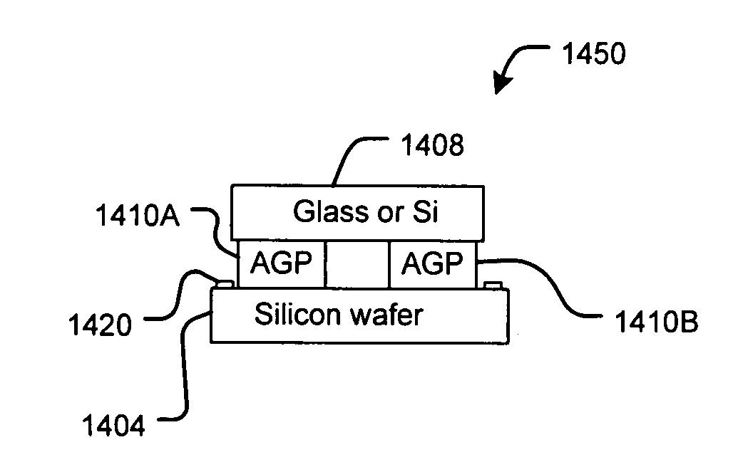
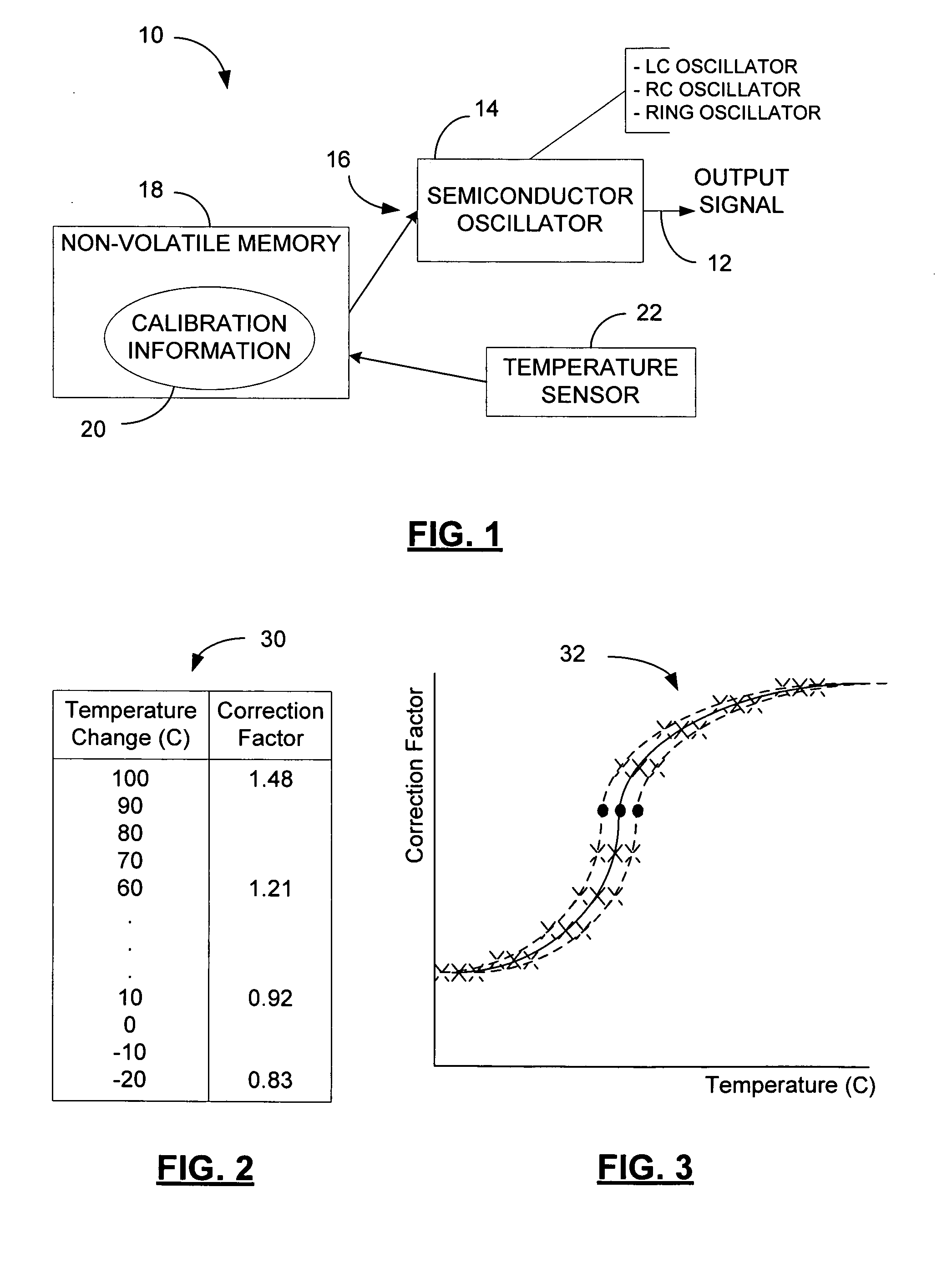
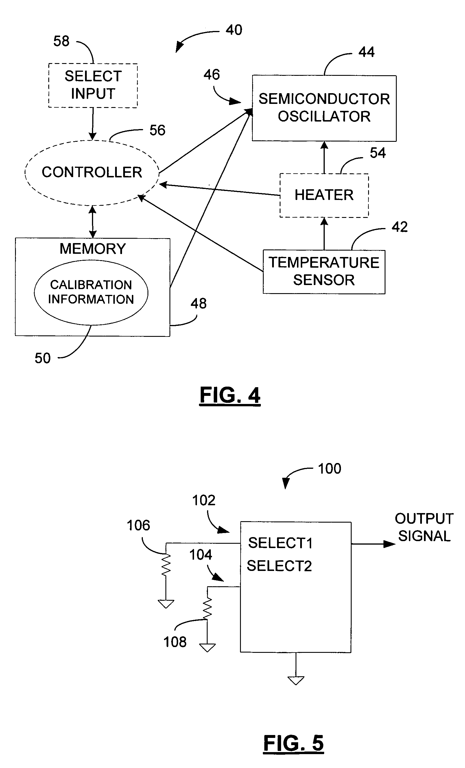
[0096]FIG. 1 shows an aspect of a crystal oscillator emulator 10 for generating an output signal 12 having a precise frequency. The crystal oscillator emulator 10 may be constructed on a single semiconductor die using any process including a Complementary-Metal-Oxide-Semiconductor (CMOS) process.

[0097] The crystal oscillator emulator 10 may include a semiconductor oscillator 14 to generate the output signal 12. Any type of semiconductor oscillator may be used including LC oscillators, RC oscillators, and ring oscillators. The semiconductor oscillator 12 includes a control input 16 to vary the frequency of the output signal. The control input 16 may be any electrical input that effects a controlled change in the output signal frequency such as the supply voltage of a ring oscillator and a voltage input to a varactor of an LC oscillator.

[0098] A non-volatile memory 18 includes calibrat...


PUM


Abstract

An integrated circuit package comprises an integrated circuit that comprises a temperature sensor that senses a temperature of the integrated circuit. A memory module stores data relating to oscillator calibrations and selects one of the oscillator calibrations as a function of the sensed temperature. An oscillator module generates a reference signal having a frequency that is based on the selected one of the oscillator calibrations. A packaging material encases at least part of the integrated circuit and has a low dielectric loss.

Description

CROSS-REFERENCE TO RELATED APPLICATIONS [0001] This application is a Continuation of U.S. patent application Ser. No. 11 / 328,979 filed Jan. 10, 2006, which claims the benefit of U.S. Provisional Application Nos. 60 / 756,828, filed Jan. 6, 2006, 60 / 714,454, filed on Sep. 6, 2005, and 60 / 730,568, filed on Oct. 27, 2005, and is a continuation-in-part of U.S. patent application Ser. No. 10 / 892,709, filed on Jul. 16, 2004, which is a continuation in part of U.S. patent application Ser. No. 10 / 272,247, filed on Oct. 15, 2002, the contents of which are hereby incorporated by reference in their entirety.TECHNICAL FIELD [0002] This invention relates to integrated circuits, and more particularly to integrated circuits with annealed glass paste arranged on a silicon wafer. BACKGROUND [0003] Precision frequency references are required in many types of electronic devices such as cellular phones and other handheld devices. Crystal oscillators are typically used to provide the precision frequency r...

Claims


Application Information

Patent Timeline
IPC IPC(8): H01L23/06
CPCG11C5/00H01L2224/49175H01L23/10H01L23/315H01L23/345H01L23/5227H01L2924/19041H01L2924/3011H03B5/04H03B5/36H03L1/026H03L1/027H03L1/04H03L7/07H03L7/0891H03L7/099H03L7/1976H01L2924/30107G11C5/143H01L2224/48247H01L2924/00H01L2224/05553
Inventor SUTARDJA, SEHAT
Owner MARVELL ASIA PTE LTD
Why Eureka
Try Eureka