Arrangement for an Organic Pin-Type Light-Emitting Diode and Method for Manufacturing

a light-emitting diode and organic technology, applied in the direction of discharge tube luminescnet screen, discharge tube/lamp details, electric discharge lamps, etc., can solve the problem of not necessarily the case, negative effect on the quantum yield of electroluminescence, and the inability to prevent possible exciplex formation, etc. problem, to achieve the effect of simplifying processing, facilitating quality assurance, and reducing investment and consumption costs for manufacturing plants

Active Publication Date: 2006-11-09
NOVALED GMBH
View PDF7 Cites 85 Cited by
  • Summary
  • Abstract
  • Description
  • Claims
  • Application Information

AI Technical Summary

Benefits of technology

[0014] The task of the invention is to state and present an arrangement for an organic pin-type light-emitting diode and a method for manufacturing, where the structural configuration of the stack of organic layers is simplified.
[0019] With such an arrangement the overall number of adopted organic matrix materials and the number of layers are reduced by the fact that, in addition to the formation of several layers of the stack of organic layers, namely the emission layer, of the doped charge carrier transport layer and the further doped charge carrier transport layer from one and the same matrix material, block layers are saved.
[0024] One advantage of the invention lies in the fact that the realisation of layer arrangements for pin-type OLEDs is enabled, which consist of less layers and / or less organic matrix materials than conventional layer arrangements. In a simplified structural element configuration the number of the adopted organic matrix materials and the adopted layers is limited where one and the same organic matrix material is used for several functional layers. This approach facilitates the quality assurance based on non-complicated processability and reliable manufacturing of OLED structural elements. In addition, investment and consumption costs for manufacturing plants can be minimised.
[0025] In addition to the substantially simplified processing, the limited number of required materials is also an advantage of the invention. Moreover, the manufacturing process is simplified be cause a reduction of the number of the sources required for layer separation is possible. When several organic layers in series are formed by one and the same organic matrix material, the manufacturing process is simplified as a result. For example, in one preferred embodiment the evaporating source for this matrix material can be continually operated, where, in each case, the source shadowing of the sources for the additional substances has to be opened for a short period of time only.

Problems solved by technology

Further examinations, related hereto, of such doped structural elements have shown, however, that this is not necessarily the case.
In the original pin-structure, exciplex formation as well as the so-called luminescence quenching effects cannot be ruled out, and this has a negative effect on the quantum yield of the electroluminescence.
With this known system, however, the possible exciplex formation is not prevented because of a decisive energy level difference between LUMO of BPhen and the HOMO of the matrix used for the emission zone.
In particular, the known system is not compatible with the combination of emitter materials selected at that location.

Method used


Image

  • Arrangement for an Organic Pin-Type Light-Emitting Diode and Method for Manufacturing
  • Arrangement for an Organic Pin-Type Light-Emitting Diode and Method for Manufacturing
  • Arrangement for an Organic Pin-Type Light-Emitting Diode and Method for Manufacturing

Examples


Embodiment Construction

[0028] The invention is described as follows in greater detail on the basis of embodiment examples with reference to the Figures of the drawing. These Figures shows the following:

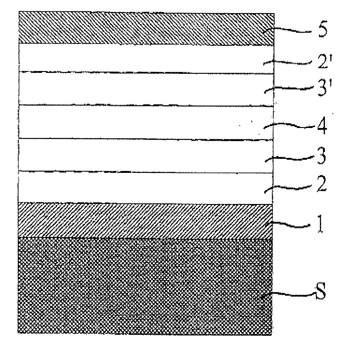
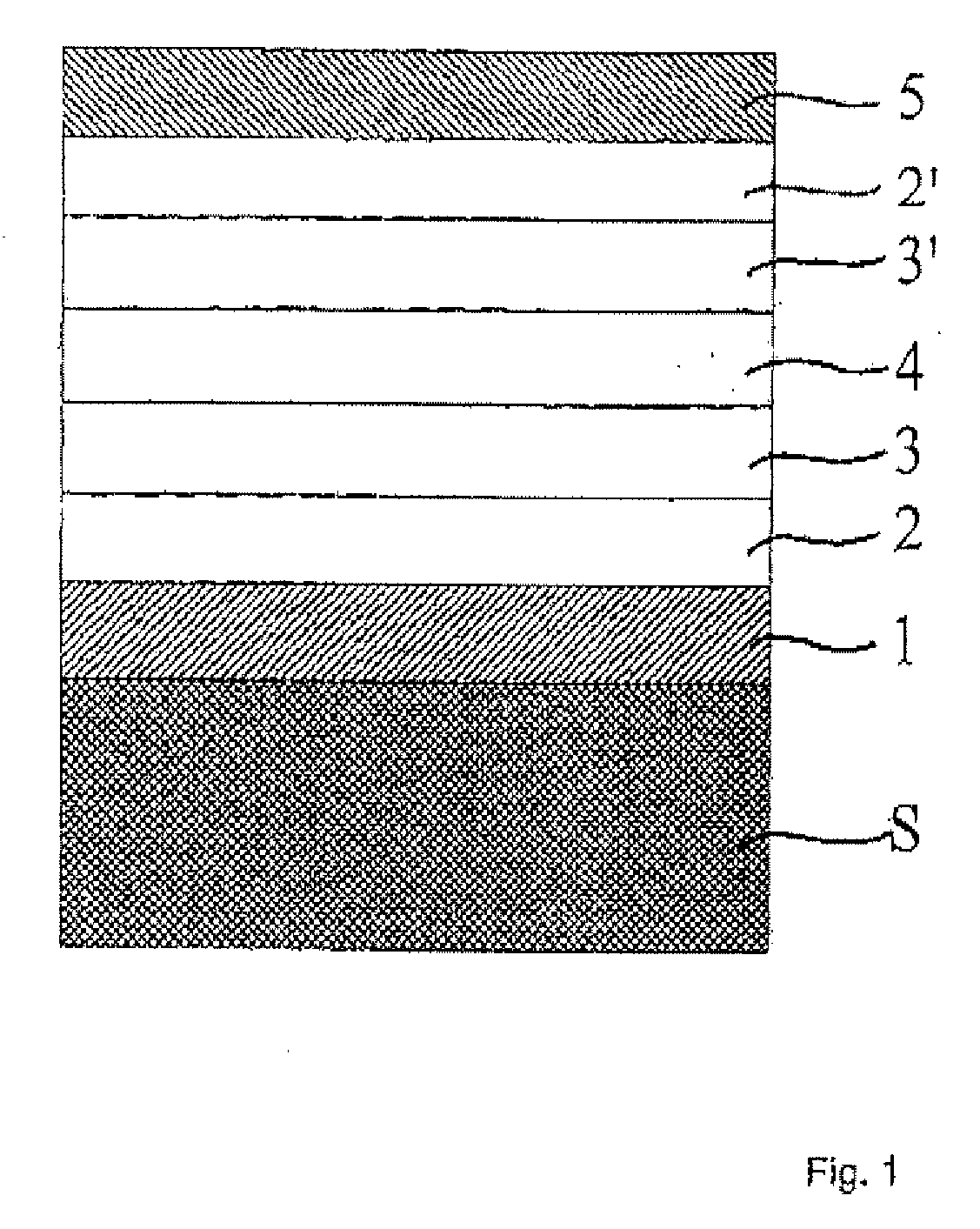
[0029]FIG. 1 a schematic illustration of a layer arrangement for a light-emitting structural element with multiple layers;

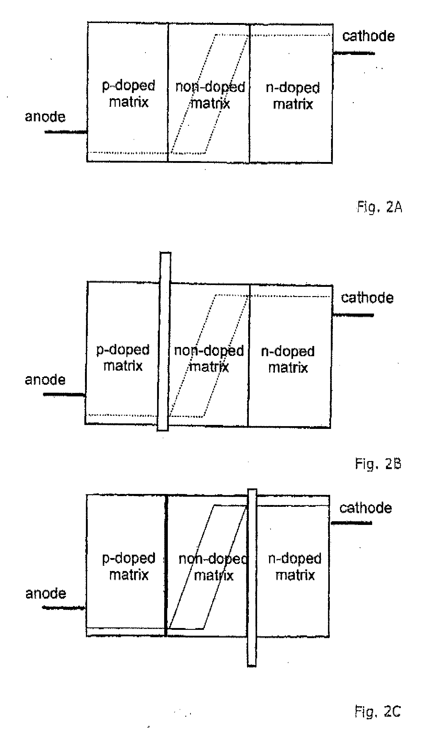
[0030]FIG. 2A to 2C schematic illustrations of energy levels for an arrangement of organic layers where at least two adjacent layers are made from the same organic matrix material;

[0031]FIGS. 3A and 3B a graphic illustration of characteristic data for the current density and the luminance as well as the current efficiency and the performance efficiency of a structural element on the basis of a structure according to an embodiment c′);

[0032]FIGS. 4A and 4B a graphic illustration of characteristic data for the current density and the luminance as well as the current efficiency and the performance efficiency of a structural element on the basis of a structure according to an embodiment ...


PUM


Abstract

The invention relates to an arrangement for an organic pin-type light-emitting diode with an electrode and a counter-electrode and a stack with organic layers between the electrode and the counter-electrode, where the stack with the organic layers comprises an emission layer comprising a k (k=1, 2, 3, . . . ) organic matrix materials, a doped charge carrier transport layer, which is arranged between the electrode and the emission layer, a further doped charge carrier transport layer, which is arranged between the counter-electrode and the emission layer, and one block layer, which is arranged between one of the doped charge carrier transport layers and the emission layer. The organic layers of the stack are formed by means of n (n≦k+2) organic matrix materials, where the n organic matrix materials comprise the k organic matrix materials of the emission layer. The stack with the organic layers can also be executed in a block-layer-free manner, where then the emission layer and the doped charge carrier transport layer are formed from an organic matrix material. Furthermore, a method for manufacturing such arrangements is stated.

Description

[0001] The invention relates to an arrangement for an organic pin-type light-emitting diode (OLED) and a method for manufacturing. BACKGROUND OF THE INVENTION [0002] Since the demonstration of low working voltages by Tang et al. (compare C. W. Tang et al.: Appl. Phys. Lett. 51 (12), 913 (1987)), organic light-emitting diodes have become promising candidates for the realisation of novel illuminating or display elements. They comprise a series of thin layers of organic materials which are preferably vapour-deposited in a vacuum or spin-coated in their polymer form. Following electric contacting by means of metal layers, they form a variety of electronic or optoelectric structural elements such as diodes, light-emitting diodes, photodiodes and transistors. With their respective properties, they provide for competition for the established structural elements on the basis of inorganic layers. [0003] In the case of the organic light-emitting diodes, and by means of the injection of charge...

Claims


Application Information

Patent Timeline
Patent Type & Authority Applications(United States)
IPC IPC(8): H05B33/14H01L51/50
CPCH01L51/002H01L51/5052H01L51/5004H10K71/30H10K50/11H10K2101/40H10K50/155H10K50/165H10K50/18H05B33/22
Inventor HOFMANN, MICHAELBIRNSTOCK, JANBLOCHWITZ-NIMOTH, JANWERNER, ANSGARPFEIFFER, MARTINHARADA, KENTARO
Owner NOVALED GMBH
Why Eureka
Try Eureka