Thin film phase-change memory

a phase-change memory and thin film technology, applied in the field of thin film phase-change memories, can solve the problems of difficult material placement into ultra-small holes, difficult to drive chalcogenide phase-change memories, and difficult to drive cmos circuits, etc., to achieve the effect of reducing current requirements, reducing cross-sectional area, and being easy to driv

Active Publication Date: 2006-11-16
MACRONIX INT CO LTD
View PDF5 Cites 55 Cited by
  • Summary
  • Abstract
  • Description
  • Claims
  • Application Information

AI Technical Summary

Benefits of technology

[0009] Briefly, in accordance with an aspect of the present invention, a thin film process and an iso-etching process are used to define a cross-sectional area of a chalcogenide memory cell. Therefore, the cross-sectional area need no longer be limited by lithography. The placement of materials into ultra small holes may also be vitiated. Moreover, the chalcogenide memory cell has a cross-sectional area that is ultra small, and, as a result, the chalcogenide memory cell can have a dramatically decreased current / power requirement.
[0010] In accordance with another aspect of the present invention, a novel memory cell and process flow fabricates a chalcogenide phase change memory (i.e., the chalcogenide memory cell). With this novel memory cell and process, the cross-sectional area of the chalcogenide memory cell can be ultra small. The cross-sectional area of the chalcogenide memory cell is defined by a chalcogenide film thickness. An iso-etch process is another one of several photo / iso-etching processes that collectively define the cross-sectional area of the chalcogenide memory cell. The extra iso-etch process decreases a width of the chalcogenide memory. Thus, the cross-sectional area can be reduced, to thereby commensurately reduce a current / power requirement of the chalcogenide phase-change memory.
[0011] In accordance with yet another aspect of the present invention, a chalcogenide memory cell having a cross-sectional area that is ultra small can be relatively easily fabricated, since there is no need to place materials into small pores (i.e., ultra small holes).

Problems solved by technology

Chalcogenide phase-change memories are not easily driven by CMOS circuits.
However, these efforts can be limited by lithography.
Furthermore, it can be difficult to place materials into ultra small holes.
Therefore, the pore size can be limited by lithography.
Accordingly, the pore size can be difficult to scale down.
Also, the size uniformity of the ultra small pores can be difficult to control.
Moreover, as previously alluded, it can be difficult to place chalcogenide into the holes.
Therefore, the pore size is basically limited by lithography and can be scaled down only with difficulty.
The electrode may be very weak because the current flow in the electrode is very high.

Method used


Image

  • Thin film phase-change memory
  • Thin film phase-change memory
  • Thin film phase-change memory

Examples


first embodiment

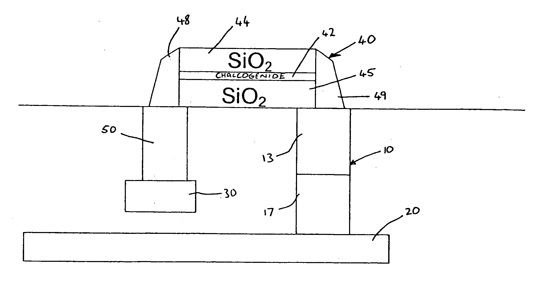
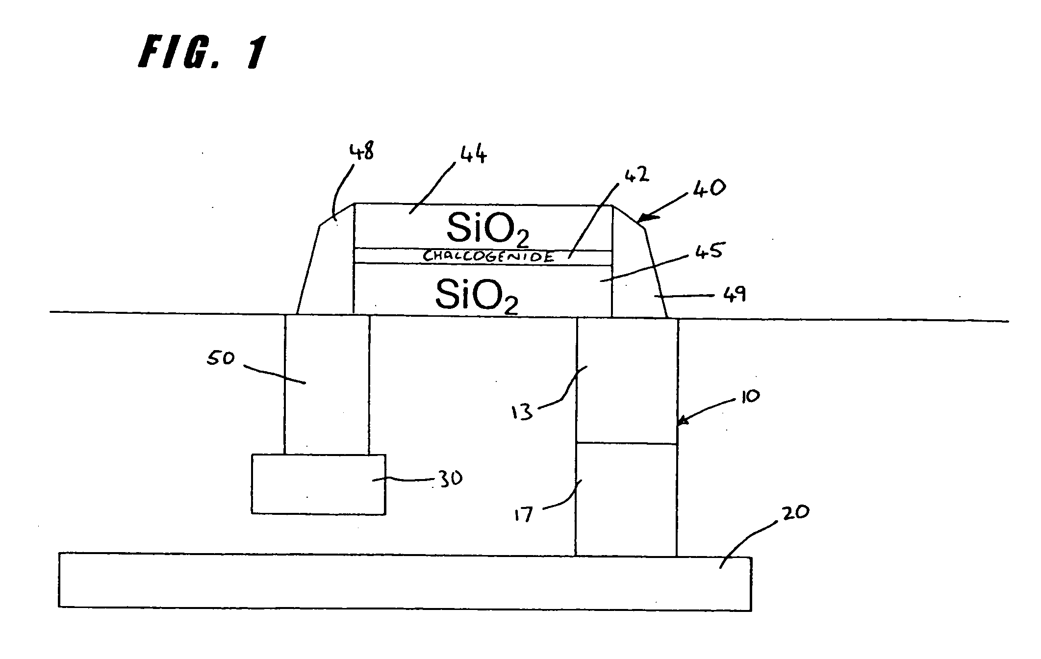
[0036]FIG. 1 illustrates how the chalcogenide memory cell of the present invention addresses these problems, wherein the chalcogenide structure 42 is implemented horizontally, rather than vertically. The chalcogenide structure 42 has an arbitrary length that is completely controllable without requiring, for example, thick layers of silicon dioxide. Instead of tapering down through a pore in the silicon dioxide layer, the chalcogenide structure 42 has a cross-sectional area that can be relatively consistent throughout the length of the chalcogenide structure 42.

[0037] This thin film process of chalcogenide deposition can result in a thin horizontal chalcogenide layer that may be not only thinner than vertical pores lithographically achievable through silicon dioxide, but also relatively uniform. The iso-etching process can create a relatively narrow horizontal chalcogenide structure 42, which can be narrower than that achievable though vertical pores of silicon-dioxide lithography. C...

third embodiment

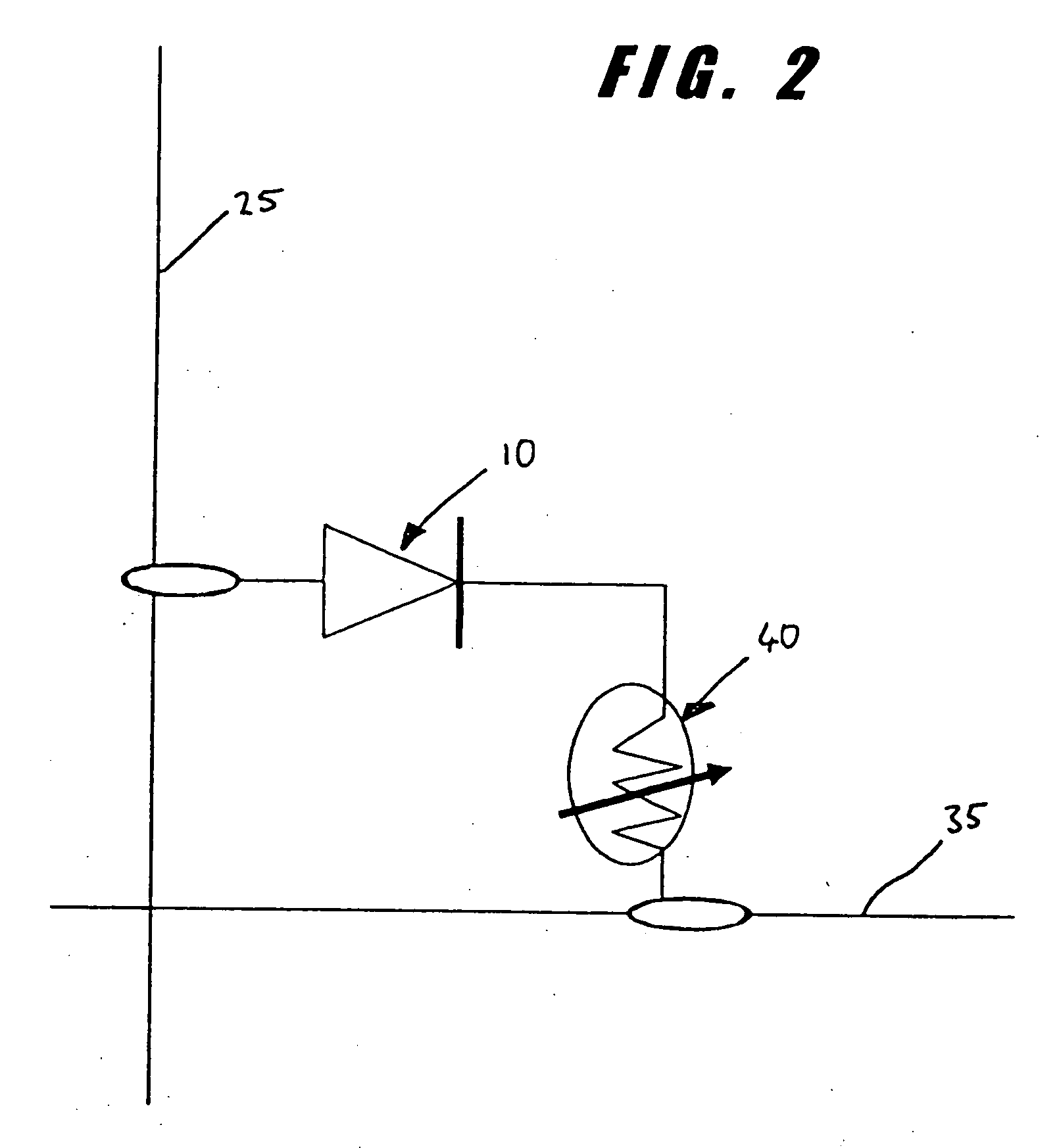
[0064]FIG. 7 is a schematic diagram depicting a chalcogenide memory cell 240, in accordance with the present invention as depicted in FIG. 6. The selecting transistor 220 is used to select the current through the chalcogenide memory cell 240. The word line 225, controlled by a CMOS circuit (not shown), does not have to carry currents large enough to write to a chalcogenide memory cell 240. The word line 225 need only carry the negligible current necessary to switch the selecting transistor 220 on.

[0065] As shown in FIG. 7, the current that is used to write to the chalcogenide memory cell 240 is obtained from a drive line 265, not from the word line as in the previous embodiments of the present invention. The drive line 265 is, for example, obtained from a current buffer (not shown) that is capable of generating relatively large currents. The drive line 265 provides a current that passes through the selecting transistor 220 to the chalcogenide memory cell 240 when the word line 225 h...

fourth embodiment

[0069]FIG. 13A is a top plan schematic representation of a cell formation flow process, and FIG. 13B is a cross-sectional view of FIG. 13A, in accordance with the present invention. In a first step, a tungsten plug structure 310 is implemented on a silicon dioxide substrate. The tungsten structure may be another structure, such as a p-poly structure or a diode. In a second step, an oxide layer / chalcogenide / oxide sandwich structure is implemented onto the result of the first step. The oxide layer may be deposited using CVD methods and the chalcogenide is deposited using sputtering methods. In a third step, the sandwich structure is patterned in accordance with photolithography (i.e., lithography) techniques. A pattern is etched in the oxide layer. The pattern need not be deep, since only shallow trenches are desired in a preferred embodiment. In a fourth step, the chalcogenide layer is iso-etched, removing substantially all of the chalcogenide except where the chalcogenide is placed ...


PUM


Abstract

A memory cell comprises a chalcogenide random access memory (CRAM) cell and a CMOS circuit. The CMOS circuit accesses the CRAM cell. The CRAM cell has a cross-sectional area that is determined by a thin film process (e.g., a chalcogenide deposition thin film process) and by an iso-etching process. If desired, the chalcogenide structure may be implemented in series with a semiconductor device such as a diode or a selecting transistor. The diode drives a current through the chalcogenide structure. The selecting transistor drives a current through the chalcogenide structure when enabled by a voltage at a gate terminal of the selecting transistor. The selecting transistor has a gate terminal, a source terminal, and a drain terminal; the gate terminal may be operatively coupled to a word line of a memory array, the source terminal may be operatively coupled to a drive line of the memory array, and the drain terminal may be operatively coupled to a bit line of the memory array.

Description

CROSS-REFERENCE TO RELATED APPLICATIONS [0001] This application is a divisional of U.S. application Ser. No. 10 / 764,750, filed Jan. 26, 2004, the entire contents of which are hereby incorporated by reference.BACKGROUND OF THE INVENTION [0002] 1. Field of the Invention [0003] The present invention relates generally to chalcogenide memories and, more particularly, to thin film phase-change memories. [0004] 2. Description of Related Art [0005] Chalcogenide phase-change memories are not easily driven by CMOS circuits. The chemical compounds known as chalcogenides generally require relatively high currents (or, more specifically, current densities) before undergoing a change of phase. Reducing the cross-sectional area of the chalcogenide or electrode can reduce the current requirement directly. Many structures have been proposed to reduce area, for example, by fabricating an ultra small contact and placing the chalcogenide into the contact. However, these efforts can be limited by lithog...

Claims


Application Information

Patent Timeline
Patent Type & Authority Applications(United States)
IPC IPC(8): H01L21/8238H01L27/10G11C13/00H01L27/105H01L27/24H01L45/00
CPCG11C13/0004G11C13/0069G11C2013/0071G11C2013/0078G11C2213/72G11C2213/79H01L27/2463H01L45/1226H01L45/1675H01L45/1691H01L27/2409H01L27/2436H01L45/06H10B63/20H10B63/30H10B63/80H10N70/823H10N70/231H10N70/068H10N70/063
Inventor LUNG, HSIANG-LANCHEN, YI-CHOU
Owner MACRONIX INT CO LTD
Why Eureka
Try Eureka