Semiconductor light-emitting device, surface-emission laser diode, and production apparatus thereof, production method, optical module and optical telecommunication system

a semiconductor and light-emitting technology, applied in the field of optical telecommunication, can solve the problems of large drive current increase, inability to construct satisfactory distributed bragg reflectors, and difficulty in constructing a surface-emission on such an inp substra

Inactive Publication Date: 2006-11-23
RICOH KK
View PDF16 Cites 33 Cited by
  • Summary
  • Abstract
  • Description
  • Claims
  • Application Information

AI Technical Summary

Benefits of technology

[0038] Accordingly, it is a general object of the present invention to provide a novel and useful light-emitting semiconductor device and fabrication process thereof wherein the foregoing problems are eliminated.

Problems solved by technology

On the other hand, conventional laser diode of the 1.3 μm band thus constructed on the InP substrate has suffered from the problem of large increase of drive current, by the factor of three times or more, when the environmental temperature has increased from room temperature to 80□.
Further, there has been a problem in that no satisfactory distributed Bragg reflector could be constructed on an InP substrate, and thus, it has been difficult to construct a surface-emission on such an InP substrate.
However, such a construction becomes inevitably expensive and has an obvious problem of poor efficiency of production.
Thus, the growth process of high quality GaInNAs layer becomes the key issue in the fabrication of such a surface-emission laser diode operable at the wavelength band of 1.3-1.55 μm.
On the other hand, the MBE process has a drawback in view of the need of high vacuum state in that it is not possible to increase the supply rate of the source materials.
When the supply rate of the source materials is increased, the load of the evacuation system becomes excessively large, and the system would undergo frequent failure or need frequent maintenance operations.
Thus, the MBE process inherently suffers from low throughput.
On the other hand, there is a report that there can be caused a degradation of efficiency of optical emission in the GaInNAs active layer provided on an Al-containing semiconductor layer even in such a case in which an intermediate layer free from Al and N is interposed between the Al-containing semiconductor layer and the GaInNAs active layer.
Associated with such a degradation of quality of the GaInNAs layer, the laser diode that uses such a GaInNAs layer suffers from the problem of poor threshold characteristics characterized by a large threshold current, which can become twice as large as the threshold current for the case in which the same active layer is formed on a GaInP cladding layer.

Method used


Image

  • Semiconductor light-emitting device, surface-emission laser diode, and production apparatus thereof, production method, optical module and optical telecommunication system
  • Semiconductor light-emitting device, surface-emission laser diode, and production apparatus thereof, production method, optical module and optical telecommunication system
  • Semiconductor light-emitting device, surface-emission laser diode, and production apparatus thereof, production method, optical module and optical telecommunication system

Examples


embodiment 1

[0277]FIG. 12 shows the construction of a laser diode according to Embodiment 1 of the present invention.

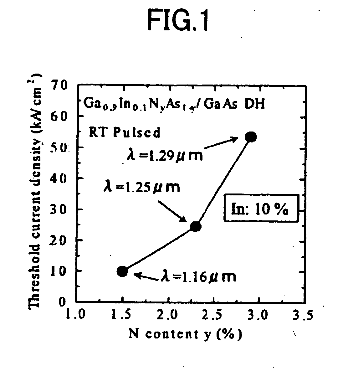
[0278] Referring to FIG. 12, the laser diode is constructed on a GaAs substrate 901 of n-type and includes a buffer layer 902 of n-type GaAs formed on the substrate 901, a cladding layer 903 of n-type AlGaAs having a composition of Al0.4Ga0.6As formed on the buffer layer 902, a first lower optical waveguide layer 904 of GaAs formed on the AlGaAs cladding layer 903 and a second lower optical waveguide layer 905 of GaAs formed on the optical waveguide layer 904, and an active layer 906 of GaInNAs / GaAs multiple quantum well structure is formed on the second lower optical waveguide layer 905.

[0279] On the active layer 906, an upper optical waveguide layer 907 of GaAs is formed and a cladding layer 908 of p-type AlGaAs having the composition of Al0.4Ga0.6As is formed on the upper optical waveguide layer 907. Further, a contact layer 909 of p-type GaAs is formed on the cladding layer...

embodiment 2

[0287]FIG. 13 shows the construction of a surface-emission laser diode according to Embodiment 2 of the present invention, wherein those parts corresponding to the parts described previously are designated by the same reference numerals and the description thereof will be omitted.

[0288] Referring to FIG. 13, the surface-emission laser diode is constructed on the GaAs substrate 901 of n-type and includes a semiconductor multilayer reflector 1001 of n-type formed on the substrate 901, wherein a first lower spacer layer 1002 of GaAs is formed on the reflector 1001 and a second lower spacer layer 1003 of GaAs is formed further on the first lower spacer layer 1002. The nitrogen-containing active layer 906 of GaInNAs / GaAs multiple quantum well structure is formed on the second lower spacer layer 1003, and an upper spacer layer 1004 of GaAs is formed on the active layer 906. Further, an AlAs selective oxidation layer 1005 is formed on the upper spacer layer 1004 and a p-type semiconductor...

embodiment 3

[0299]FIG. 14 shows the construction of a surface-emission laser diode according to Embodiment 3 of the present invention, wherein those parts corresponding to the parts described previously are designated by the same reference numerals and the description thereof will be omitted.

[0300] Referring to FIG. 14, the laser diode of Embodiment 3 has a construction similar to that of the laser diode of Embodiment 2 except that the entire layers from the lower spacer layer 1101 to the upper spacer layer 1104 form an Nλ optical cavity (N=2, 3, 4, . . . ). Thus, the lower spacer layer 1101 has a thickness db determined as

db=(N−0.5)λ / ns−(na / ns)(da / 2)

wherein λ represents the laser oscillation wavelength, ns represents the refractive index of the GaAs spacer layer, na represents the refractive index of the active layer, and da represents the thickness of the active layer. Further, the upper spacer layer 1004 has a thickness du determined as

du=0.5λ / ns−(na / ns)(da / 2)

[0301] In the case of N=4,...


PUM


Abstract

A semiconductor light-emitting device has a semiconductor layer containing Al between a substrate and an active layer containing nitrogen, wherein Al and oxygen are removed from a growth chamber before growing said active layer and a concentration of oxygen incorporated into said active layer together with Al is set to a level such that said semiconductor light-emitting device can perform a continuous laser oscillation at room temperature.

Description

[0001] This application is a divisional application of U.S. patent application Ser. No. 10 / 878,282, filed on Jun. 29, 2004, now U.S. Pat. No. 7,067,846 issued Jun. 27, 2006, which in turn is a divisional of U.S. patent application Ser. No. 10 / 105,800, filed on Mar. 26, 2002, now U.S. Pat. No. 6,765,232 issued Jul. 20, 2004, the entirety of each of which is incorporated herein by reference. BACKGROUND OF THE INVENTION [0002] The present invention generally relates to the technology of optical telecommunication and more particularly to an optical semiconductor device such as a laser diode used in optical telecommunication systems. Especially, the present invention is related to a surface-emission laser diode and fabrication process thereof, a growth apparatus and a growth process used for forming such a surface-emission laser diode, as well as optical transmission modules, optical transceiver modules and optical telecommunication systems that use such a surface-emission laser diode. [...

Claims


Application Information

Patent Timeline
Patent Type & Authority Applications(United States)
IPC IPC(8): H01L33/00H01L33/02H01L33/10H01L33/32
CPCB82Y20/00H01S2304/04H01L33/025H01L33/10H01L33/32H01S5/0014H01S5/02284H01S5/18305H01S5/18308H01S5/18311H01S5/18341H01S5/18394H01S5/3211H01S5/32366H01S5/343H01S5/34306H01S5/34333H01L33/007H01S5/02251
Inventor TAKAHASHI, TAKASHIKAMINISHI, MORIMASASATO, SHUNICHIITOH, AKIHIROJIKUTANI, NAOTO
Owner RICOH KK
Why Eureka
Try Eureka