

Magnetic memory and method of manufacturing the memory
a technology of magnetic memory and manufacturing method, which is applied in the direction of magnetic field-controlled resistors, galvano-magnetic devices, semiconductor devices, etc., can solve the problems of deteriorating magnetic characteristics of ferromagnetic layers and inability to obtain sufficient characteristics as mrams, and achieve high yield.
- Summary
- Abstract
- Description
- Claims
- Application Information
AI Technical Summary
Benefits of technology
Problems solved by technology
Method used
Image

Examples
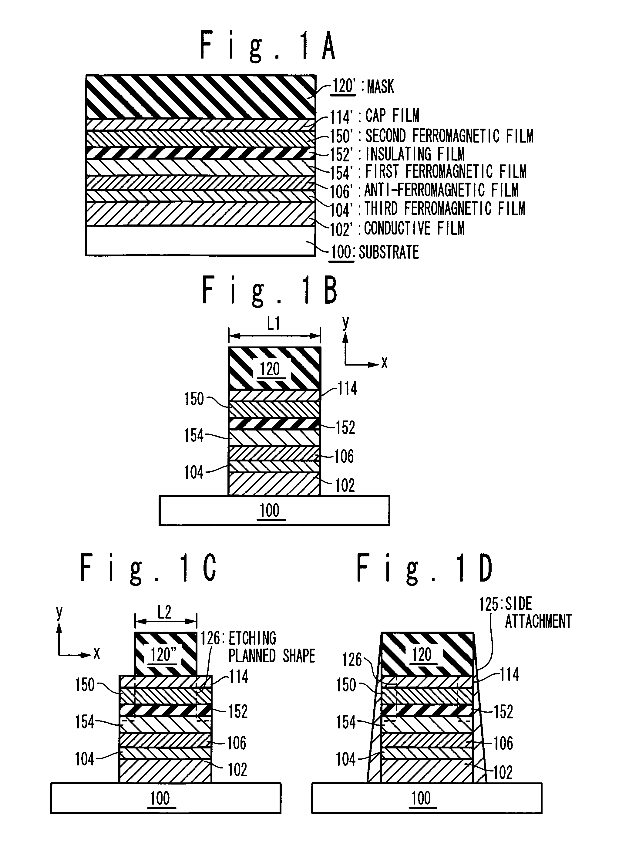
first embodiment
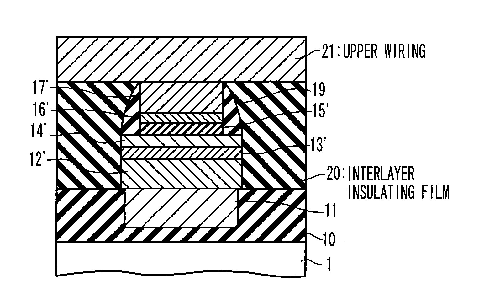
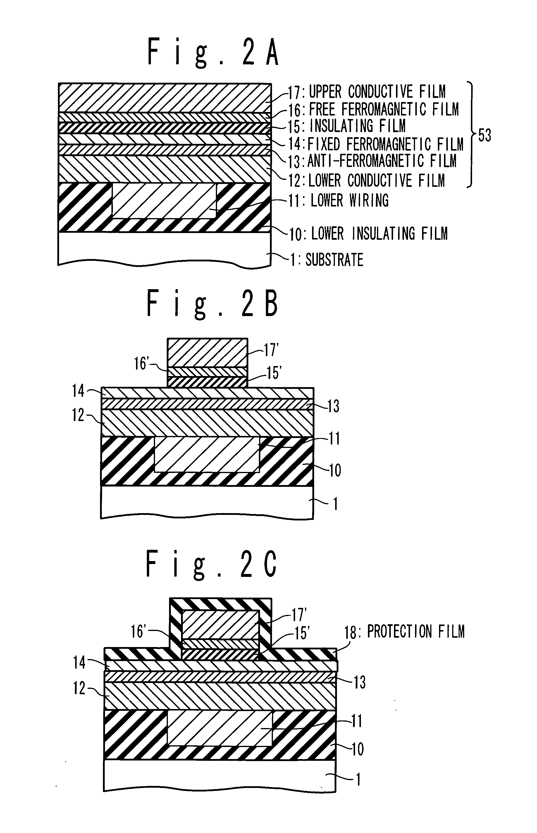
[0043] The magnetic memory according to the first embodiment of the present invention and the manufacturing method of the same will be described below. FIGS. 2A to 2F are cross sectional views showing the method of manufacturing the magnetic memory according to the first embodiment of the present invention. The magnetic memory manufacturing method in this embodiment is a method of manufacturing a TMR cell. The magnetic element serving as the TMR cell is formed on a wiring layer of copper or the like which is formed on a CMOS circuit. FIGS. 2A to 2F show steps of manufacturing the magnetic element on a lower wiring 11 made of copper or the like.
[0044] First, as shown in FIG. 2A, the lower wiring 11 (e.g., of copper) for write and read is formed in a lower insulating layer 10 (e.g., formed from a silicon oxide film) which is formed on a substrate 1 (e.g., of silicon) by using a damascene process. A multi-layer film 53 for a TMR structure is formed on the lower wiring 11. That is, a l...
second embodiment
[0064] Then, the magnetic memory and its manufacturing method according to the second embodiment of the present invention will be described below.
[0065]FIGS. 3A to 3F are cross sectional views showing a magnetic memory manufacturing method according to the second embodiment. The magnetic element manufacturing method of this embodiment is a method for manufacturing a TMR cell. The magnetic element serving as a TMR cell is formed on a via-contact made of tungsten (tungsten plug) for electrically connecting a wiring of copper or the like formed on a CMOS circuit with the magnetic element. FIGS. 3A to 3F show steps of forming the magnetic element on the tungsten plug 22 on the lower wiring 11 of copper aluminum (AlCu) or the like.
[0066] First, as shown in FIG. 3A, in the area for forming the magnetic element 54 on a lower insulating layer 10 (e.g., silicon oxide film) formed on a substrate 1 (e.g., silicon), the write and read lower wiring 11 and the tungsten plug 22 (e.g., copper alu...
third embodiment
[0085] The magnetic memory and its manufacturing method according to the third embodiment of the present invention will be described below. FIGS. 4A to 4F are cross sectional views showing the magnetic memory manufacturing method in the third embodiment of the present invention. The magnetic memory manufacturing method of this embodiment is a TMR cell manufacturing method. The magnetic element serving as the TMR cell is formed on a wiring made of copper or the like which is formed on or above a CMOS circuit. FIGS. 4A to 4F show steps of manufacturing a magnetic element formed on the lower wiring 11 made of copper or the like.
[0086] First, as shown in FIG. 4A, the lower wiring 11 (e.g., copper) for write and read is formed in the lower insulating layer 10 (e.g., silicon oxide film) formed on the substrate 1 (e.g., silicon) by using the damascene process. The multi-layer film 53′ having a TMR structure is formed on the lower wiring 11. That is, a lower conductive film 12, a free ferr...
PUM
 Abstract
Description
Claims
Application Information